

Light-emitting device, image forming apparatus, display device, and electronic apparatus
A technology for a light-emitting device and a light-emitting layer, which is applied to equipment for electric recording technology using charge patterns, electric recording technology for applying charge patterns, lighting devices, etc., and can solve problems such as deterioration of luminous characteristics of EL elements and damage to EL elements
- Summary
- Abstract
- Description
- Claims
- Application Information
AI Technical Summary
Problems solved by technology
Method used
Image

Examples
no. 1 approach
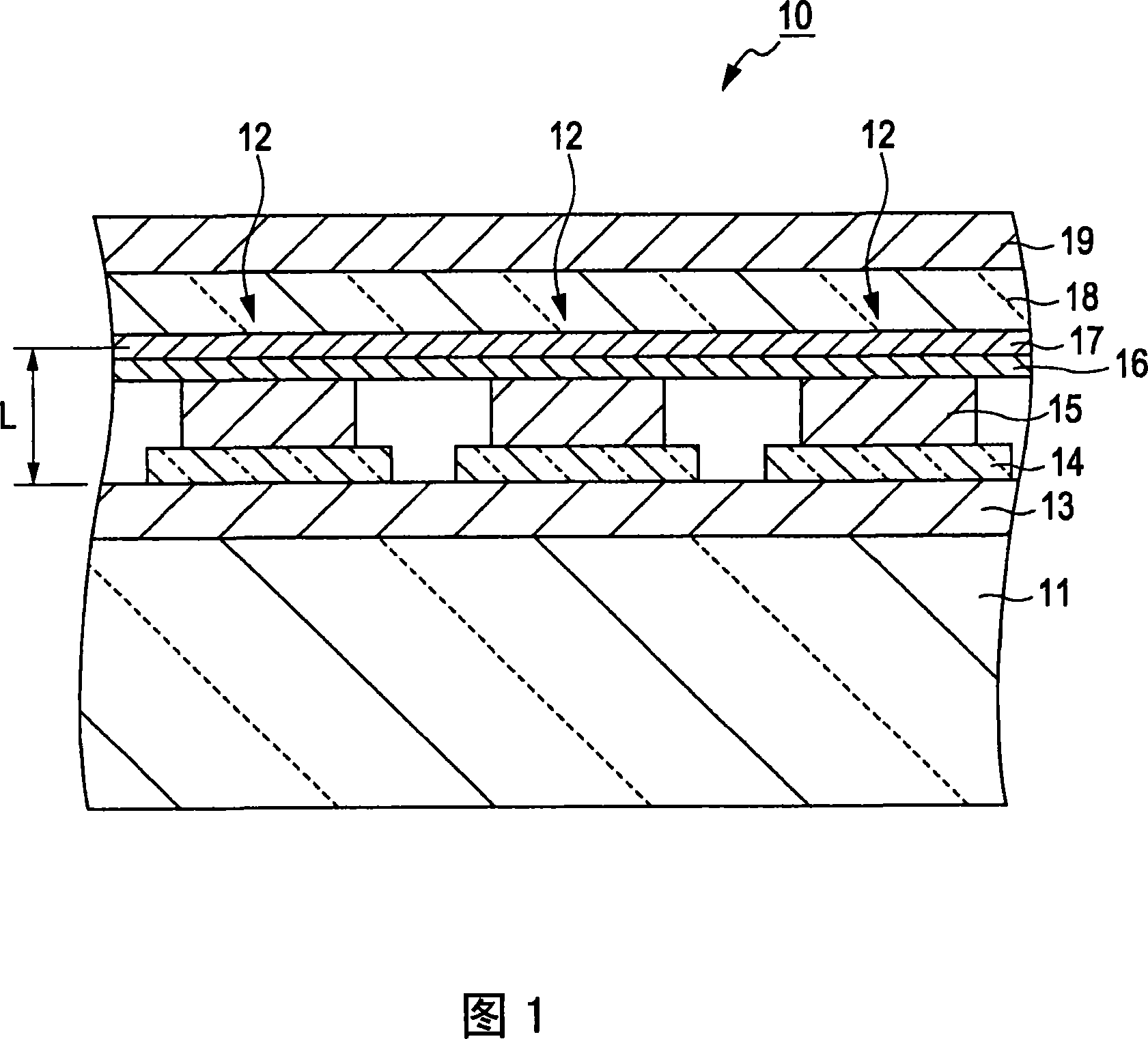
[0078] FIG. 1 is a cross-sectional view showing part of a light emitting device 10 according to a first embodiment of the present invention. This light emitting device 10 has a plurality of light emitting elements 12 arranged on a substrate. In the figure, only three light emitting elements 12 are illustrated. Each light emitting element 12 is an OLED (Organic Light Emitting Diode) element which is an organic EL element. That is, the light emitting device 10 is an organic EL device.
[0079] The substrate 11 is formed of, for example, glass, and has a thickness of, for example, 500 μm. A light reflection layer 13 that totally reflects light is formed on the substrate 11 . The light reflection layer 13 is formed of a material having a high light reflectance to resonate light, has a smooth upper surface, and has a thickness of, for example, 200 nm. The material for forming the light reflection layer 13 is specifically silver, but the present embodiment may be modified and ma...
no. 2 approach
[0101] FIG. 14 is a cross-sectional view showing part of a light emitting device 20 according to a second embodiment of the present invention. This embodiment differs from the first embodiment in that a color image can be displayed. The light-emitting device 20 is suitable for displaying color images, and has a plurality of pixels arranged in a matrix on the light-reflecting layer 23 . Each pixel has a light emitting element 22R that emits R light that is close to red, a light emitting element 22G that emits G light that is close to green, and a light emitting element 22B that emits B light that is close to blue. The structure below the light emitting elements 22R, 22G, and 22B is the same as the structure below the light emitting element 12 in the light emitting device 10 , but the light reflecting layer 23 may be provided instead of the light reflecting layer 13 . The light reflection layer 23 differs from the light reflection layer 13 only in that it is formed of aluminum....
no. 3 approach
[0117] FIG. 23 is a cross-sectional view showing part of a light emitting device 50 according to a third embodiment of the present invention. This embodiment differs from the first embodiment in that a transparent layer is arranged between the light reflection layer 13 and the transparent electrode 14 . This light emitting device 50 has a plurality of light emitting elements 52 arranged on a substrate 51 . In the drawing, three light emitting elements 52 are illustrated. Each light emitting element 52 is an OLED (Organic Light Emitting Diode) element which is an organic EL element. That is, the light emitting device 50 is an organic EL device.
[0118] The substrate 51 is formed of, for example, glass, and has a thickness of, for example, 500 μm. A light reflection layer 53 that totally reflects light is formed on the substrate 51 . The light reflection layer 53 is capable of resonating light, is formed of a material with a high light reflectance, has a smooth upper surfac...
PUM
| Property | Measurement | Unit |
|---|---|---|
| Thickness | aaaaa | aaaaa |
| Thickness | aaaaa | aaaaa |
| Thickness | aaaaa | aaaaa |
Abstract
Description
Claims
Application Information