
Method for manufacturing semiconductor chips from wafers

A technology of conductor chips and semiconductors, which is applied in the direction of semiconductor devices, semiconductor/solid-state device manufacturing, electrical components, etc., and can solve problems such as expensive costs

Active Publication Date: 2011-12-07
ROBERT BOSCH GMBH
View PDF0 Cites 0 Cited by
  • Summary
  • Abstract
  • Description
  • Claims
  • Application Information

AI Technical Summary

Problems solved by technology

However, this requires additional expensive and cost-intensive process steps

Method used


Image

  • Method for manufacturing semiconductor chips from wafers
  • Method for manufacturing semiconductor chips from wafers
  • Method for manufacturing semiconductor chips from wafers

Examples


Embodiment Construction

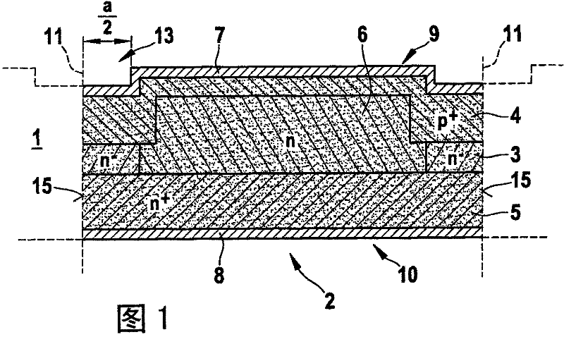
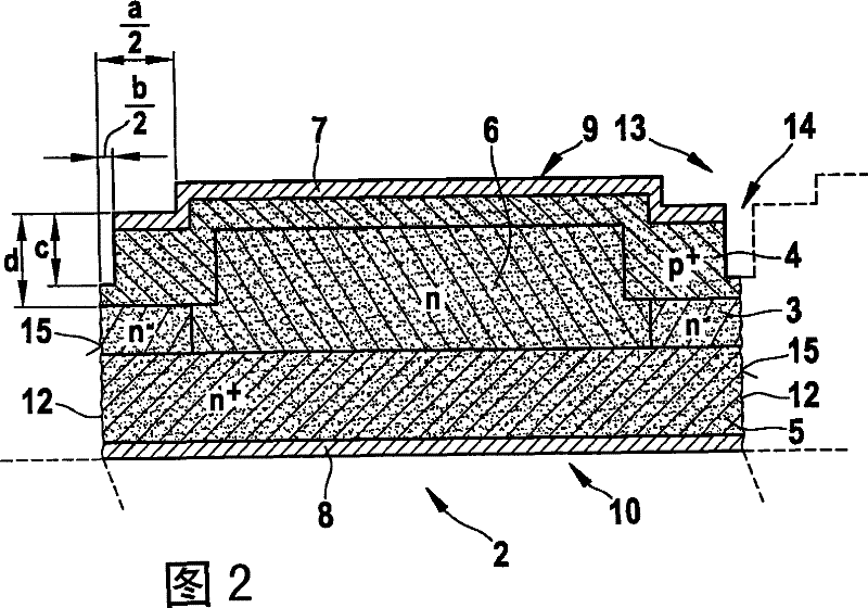
[0023] figure 1 Shown is a semiconductor chip 2 of a Zener diode (also known as a ZR diode) known from the prior art with reduced fringing field strength. The diode chip 2 is fabricated from a silicon substrate having, for example, approximately 8×10 15 cm -3 n doping. Viewed from the front side 9 to the back side 10, chip 2 contains p + Doped layer 4, an underlying n-doped substrate layer 6, which is laterally p-doped + doped layer 4 and the underlying weak n - Doped layer 3 surrounded, also has a strong n arranged on the backside 10 of the chip + Doped layer 5. In addition, a metallization layer 7 or 8 is applied to the front side 9 and the rear side 10 .

[0024] The ZR diode is distinguished in that breakdown occurs only in the center of the chip and not in the edge region of the diode chip 2 when operating in the blocking direction. This effect is due to the Zener diode having a different pn junction in the center of the diode chip 2 and on the edge 15 . In the c...


PUM


Abstract

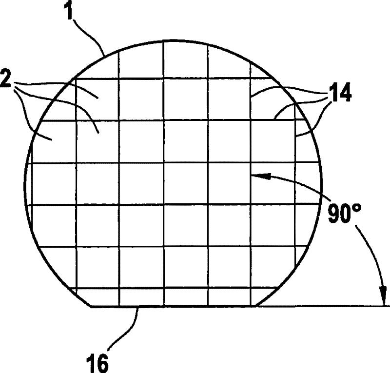
The invention relates to a method for producing semiconductor chips (2) from a wafer (1) containing a plurality of semiconductor chips (2). When given breaks (14) are produced on the wafer surface after the wafer (1) is completed, and the wafer (1) is broken along these given breaks (14) to separate the semiconductor chips (2), it is possible Defects in the crystal structure of the chip (2) are significantly reduced.

Description

technical field [0001] The invention relates to a method for producing semiconductor chips from a wafer and to a semiconductor component produced by means of the method. Background technique [0002] Semiconductor devices, such as diodes, transistors or thyristors, usually contain a semiconductor chip that is packaged in a housing. These semiconductor chips are usually manufactured from a wafer, which usually contains a very large number of identical semiconductor chips. After the wafer is complete, usually after the final metallization step, the chips are separated from the wafer. The separation of the chips is usually carried out by means of a diamond saw. This sawing process can be implemented relatively simply, but has the disadvantage of producing crystal defects along the cutting facet along the entire chip edge, which extend into the chip up to a depth of several tens of micrometers. These crystal defects are important especially in the case of devices with pn junc...

Claims


Application Information

Patent Timeline
Patent Type & Authority Patents(China)
IPC IPC(8): H01L21/78H01L29/866
CPCH01L29/866H01L21/78H01L29/66106H01L29/045
Inventor R·施皮茨A·格拉赫F·哈恩
Owner ROBERT BOSCH GMBH
Learn More