Low-voltage differential signal receiver

A receiving device, low-voltage differential technology, applied in the direction of cathode ray tube indicator, digital output to display equipment, instruments, etc., can solve the problems affecting signal transmission quality, difficulty, timing difference, etc., to improve the efficiency and quality of pixel transmission , to avoid sampling errors, the effect of consistent delay time

Inactive Publication Date: 2010-10-27
益士伯电子股份有限公司
View PDF6 Cites 0 Cited by
  • Summary
  • Abstract
  • Description
  • Claims
  • Application Information

AI Technical Summary

Problems solved by technology

[0009] The problem with current low voltage differential signaling (LVDS) receivers is that the delay time of each clock and data signal path is different due to many factors. The number, type and manufacturing process of electronic components on each path, voltage variation Factors such as these will cause different timing differences between the corresponding clock pulses and data of each group, which will easily cause sampling errors and affect the quality of signal transmission. It will become more obvious as the pixel transmission rate increases.
[0010] In order to overcome the large number of sampling errors that accompany the increase in pixel transmission rate, under the current low-voltage differential signal (LVDS) receiver architecture, it is necessary to address the number, type, manufacturing process, and voltage of electronic components with different clock pulses and data paths. Changes and other factors make corresponding adjustments in the circuit layout to take into account both the improvement of the pixel transmission rate and the quality of signal transmission. However, this requires a lot of time and effort for the manufacturer.
[0011] Therefore, under the low-voltage differential signal (LVDS) receiver architecture of the prior art, it will be very difficult to increase the pixel transmission rate and take into account the signal transmission quality.

Method used


Image

  • Low-voltage differential signal receiver
  • Low-voltage differential signal receiver
  • Low-voltage differential signal receiver

Examples


Embodiment Construction

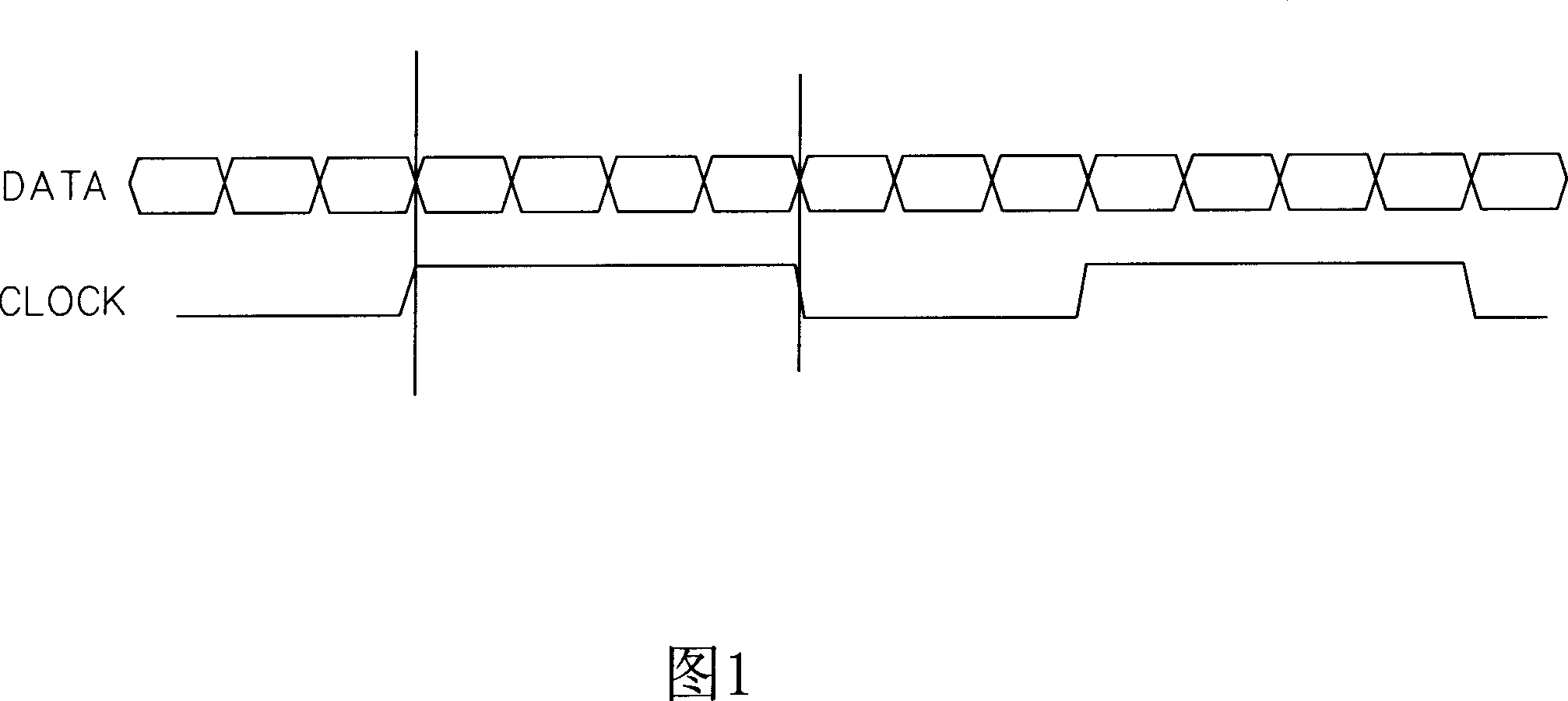
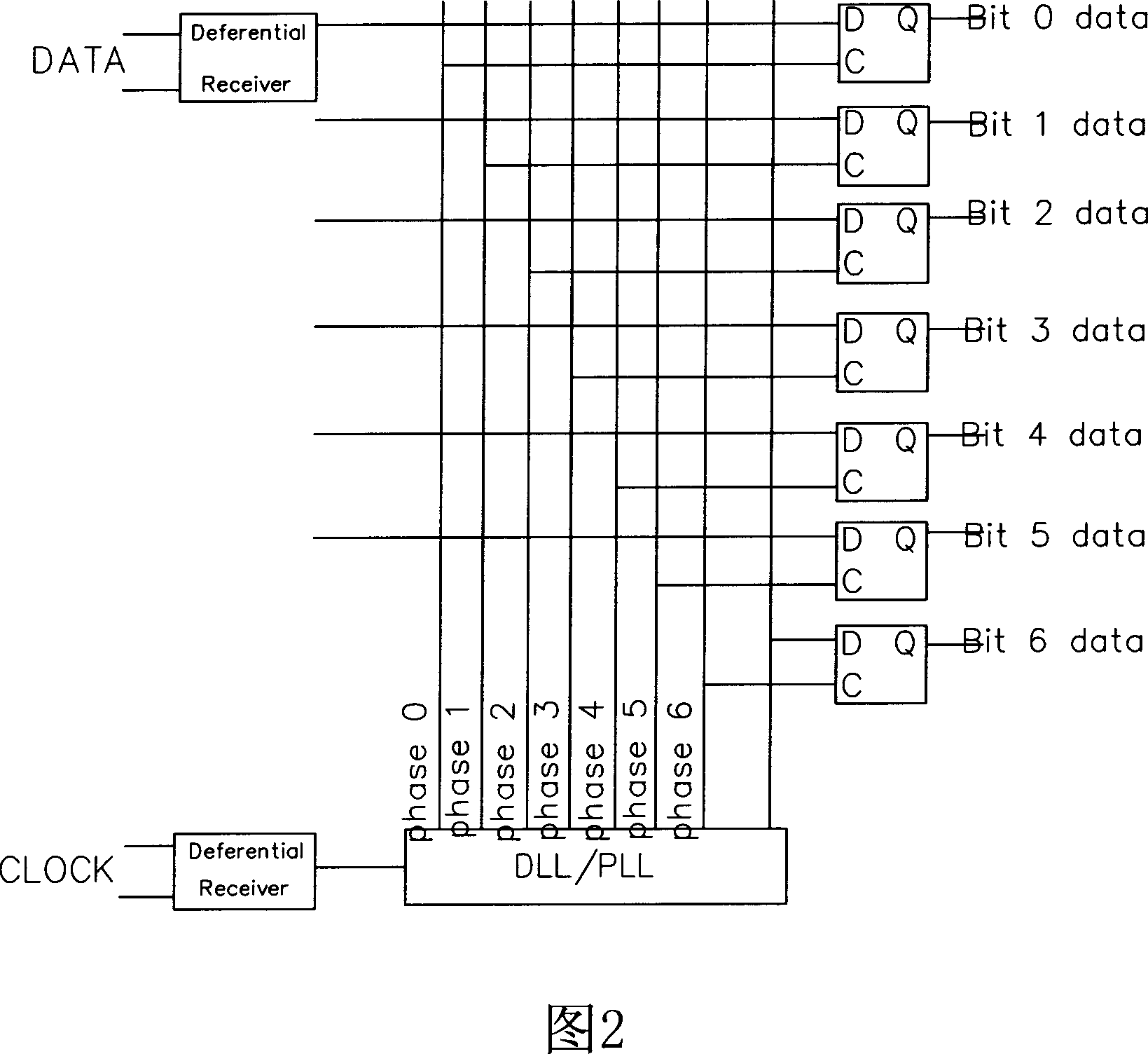
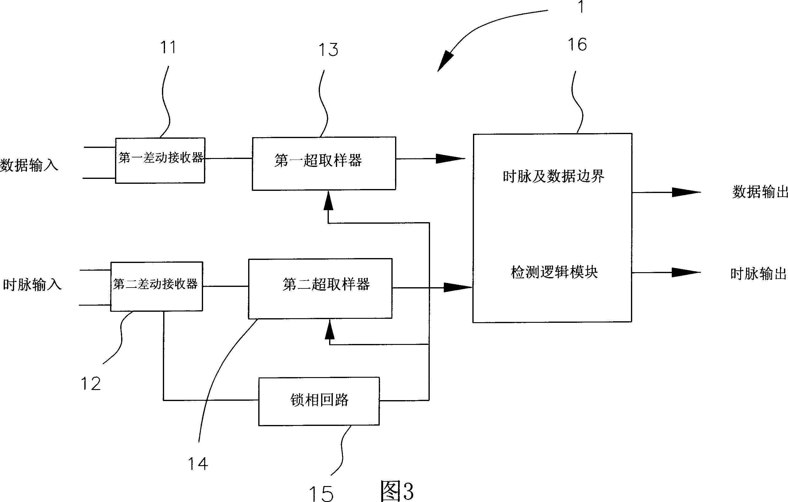
[0038] see image 3 , is an implementation structure diagram of the low voltage differential signal receiving device of the present invention. It can be seen from the figure that the low voltage differential signal (Low Voltage Differential Signal, LVDS) receiving device 1 of the present invention includes:

[0039] The first differential receiver (Differentia Receiver) 11 is to receive the data signal input from the data signal input port, and output the data signal to the first oversampling device (Oversampling) 13, and then output the data signal to the data A boundary detection logic module (Clock Edge Data Boundary Detection & Data Extraction) 16, when the data signal input port is more than one, the first differential receiver 11 and the first supersampler 13 can be set to the same number as the data signal input port multiple sets of circuits with the same purpose in order to transmit multiple data signals at the same time;

[0040] The second differential receiver 12 ...


PUM


Abstract

This device consists of two differential receivers, two super samplers, the phase-locked circuit, the clock impulse (CI) and the data margin test logic module (MTL). This invention treats the CI signal as another data signal and transfers the CI signal and the data signal via the same circuit layout path. It uses the asynchronous CI to raise the sampling frequency against input IC and data. Then it uses special IC and data MTL to verify the conversion of IC and analyzes out the data byte from the IC and data specimen. This device can effectively raise the transferring efficiency and quality of pixel.

Description

Technical field [0001] The present invention is a low -voltage signal receiving device, especially a low -voltage differential signal receiving device that can improve the quality and efficiency of the transmission of low -voltage difference (LVDS). Background technique [0002] In recent years, due to the faster and faster operation of the processor, the amount of data processing of the unit time has also increased. Therefore, the transmission of the data of computer peripheral equipment and the application of various integrated circuit products.These must be completed by an interface circuit that can be transmitted and received in large quantities.In terms of long -distance transmission of tens of kilometers or even hundreds of kilometers, optical fiber can be used as a transmission tool, but the transmission of flow fiber transmission on each tens of meters or even the circuit board, and the fiber transmission is unrealistic.Therefore, the transmission lines must be relying on...

Claims


Application Information

Patent Timeline
Patent Type & Authority Patents(China)
IPC IPC(8): G06F3/14G09G5/00
Inventor 陈永建
Owner 益士伯电子股份有限公司
Why Eureka
Try Eureka