Wafer and semiconductor device testing method

A test method, semiconductor technology, applied in the field of wafers, can solve problems such as no description or hint, and achieve the effect of reducing the number

Inactive Publication Date: 2008-01-16
SHARP KK
View PDF3 Cites 3 Cited by
  • Summary
  • Abstract
  • Description
  • Claims
  • Application Information

AI Technical Summary

Problems solved by technology

[0008] However, in said patent document, there is no description or hint at all about reducing the number of pads for testing or the number of contact pins of a probe card by reducing the number of signals for testing.
Therefore, there is room for improvement

Method used


Image

  • Wafer and semiconductor device testing method
  • Wafer and semiconductor device testing method

Examples


Embodiment Construction

[0039] Hereinafter, the present invention will be described in detail using the illustrated embodiments.

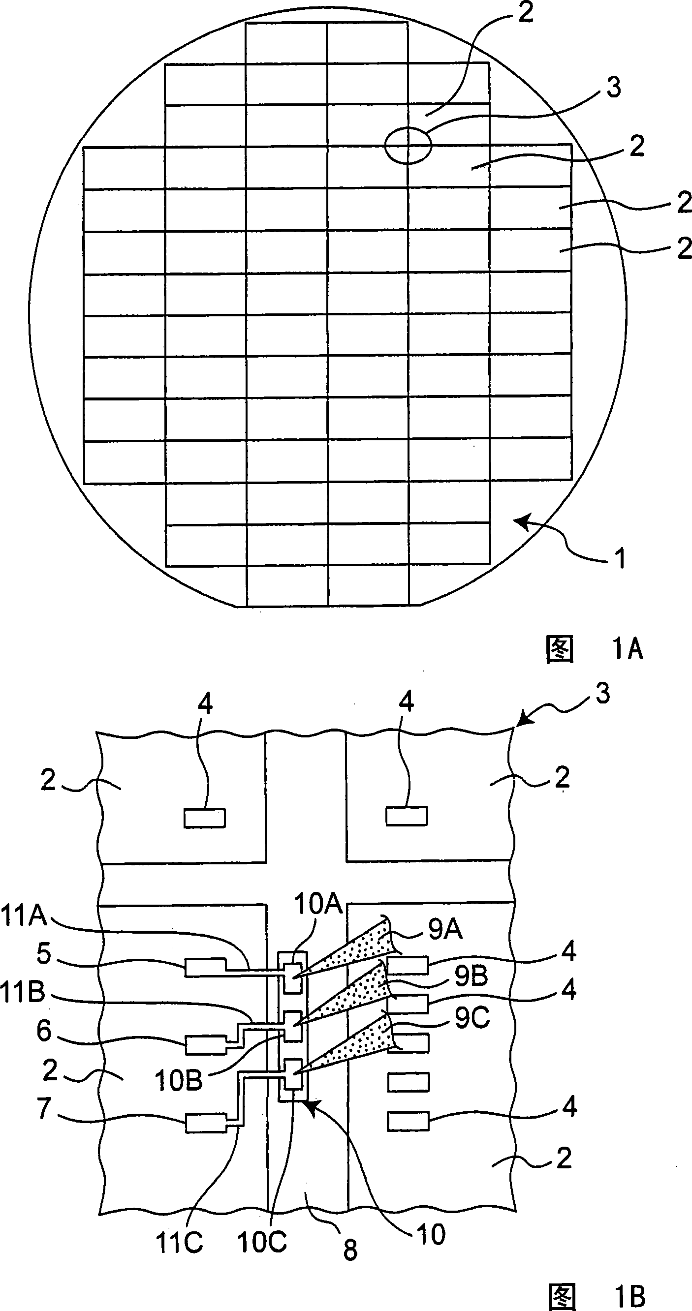
[0040]FIG. 1A shows a schematic structure of a wafer 1 according to one embodiment of the present invention. This wafer 1 is a wafer that has undergone a wafer process, and the surface of the wafer is divided into a plurality of rectangular areas (referred to as "chip areas") 2 like a general wafer. A semiconductor device (not shown) is produced in each chip region 2 .

[0041] FIG. 1B shows an enlarged portion of FIG. 1A , that is, a portion 3 where the corners of the four chip regions 2 are concentrated. As shown in FIG. 1B , chip regions 2 are separated from each other by dicing lines (also referred to as dividing lines) 8 having a fixed width. Then, after the wafer test described later is completed, the wafer 1 is divided into chips along the dicing lines 8 . A plurality of pads 4 for inputting and outputting signals between elements in the chip area and the outsid...


PUM


Abstract

At least three pads 10 A, 10 B, 10 C are provided on a scribe line 8 located adjacent to a chip region 2. The three pads are a power pad 10 A connected to a power potential portion 5 in the chip region 2, a grounding pad 10 B connected to a ground potential portion 6 in the chip region 2, and a switchover pad 10 C that is connected to a semiconductor device 7 in the chip region 2 and switches the operating state of the semiconductor device 7 between a normal operating state and a standby state. During a wafer test, contact pins 9 A, 9 B, 9 C of a probe card are brought in contact with the three pads 10 A, 10 B, 10 C, respectively.

Description

technical field [0001] The present invention relates to a wafer, and more particularly to a wafer in which a semiconductor device is formed for each chip area. [0002] Furthermore, the present invention relates to a method of testing semiconductor devices fabricated on such wafers. Background technique [0003] As shown in FIG. 2A, in a general wafer 101 that has undergone a wafer process, the wafer surface is divided into a plurality of rectangular areas (which are referred to as "chip areas") 102, and a semiconductor device is fabricated for each chip area 102 ( not shown). As shown in FIG. 2B (enlargingly showing a portion 103 in FIG. 2A ), chip regions 102 are separated from each other by dicing lines (also referred to as dividing lines) 108 having a fixed width. A plurality of pads 104 for inputting and outputting signals between elements in the chip area and the outside are arranged on the peripheral portion of each chip area 102 (portion along the dicing line 108 )...

Claims


Application Information

Patent Timeline
Patent Type & Authority Applications(China)
IPC IPC(8): H01L23/544H01L23/485H01L21/66G01R31/00G01R31/26G01R31/28
CPCG01R31/2831H01L22/32G01R31/2884H01L2224/05553H01L22/00
Inventor 藤野宏晃
Owner SHARP KK
Why Eureka
Try Eureka