
Device isolation structure used for high pressure manufacturing process and its manufacturing method

An isolation structure and device isolation technology, applied in the manufacture of the device isolation structure, shallow trench isolation mixed with local silicon oxidation isolation device structure field, can solve problems such as unfavorable process control

Inactive Publication Date: 2008-01-23
SHANGHAI HUA HONG NEC ELECTRONICS
View PDF0 Cites 0 Cited by
  • Summary
  • Abstract
  • Description
  • Claims
  • Application Information

AI Technical Summary

Problems solved by technology

This also leads to many difficulties in the realization of the STI process in the high-pressure process, which is not conducive to the final process control

Method used


Image

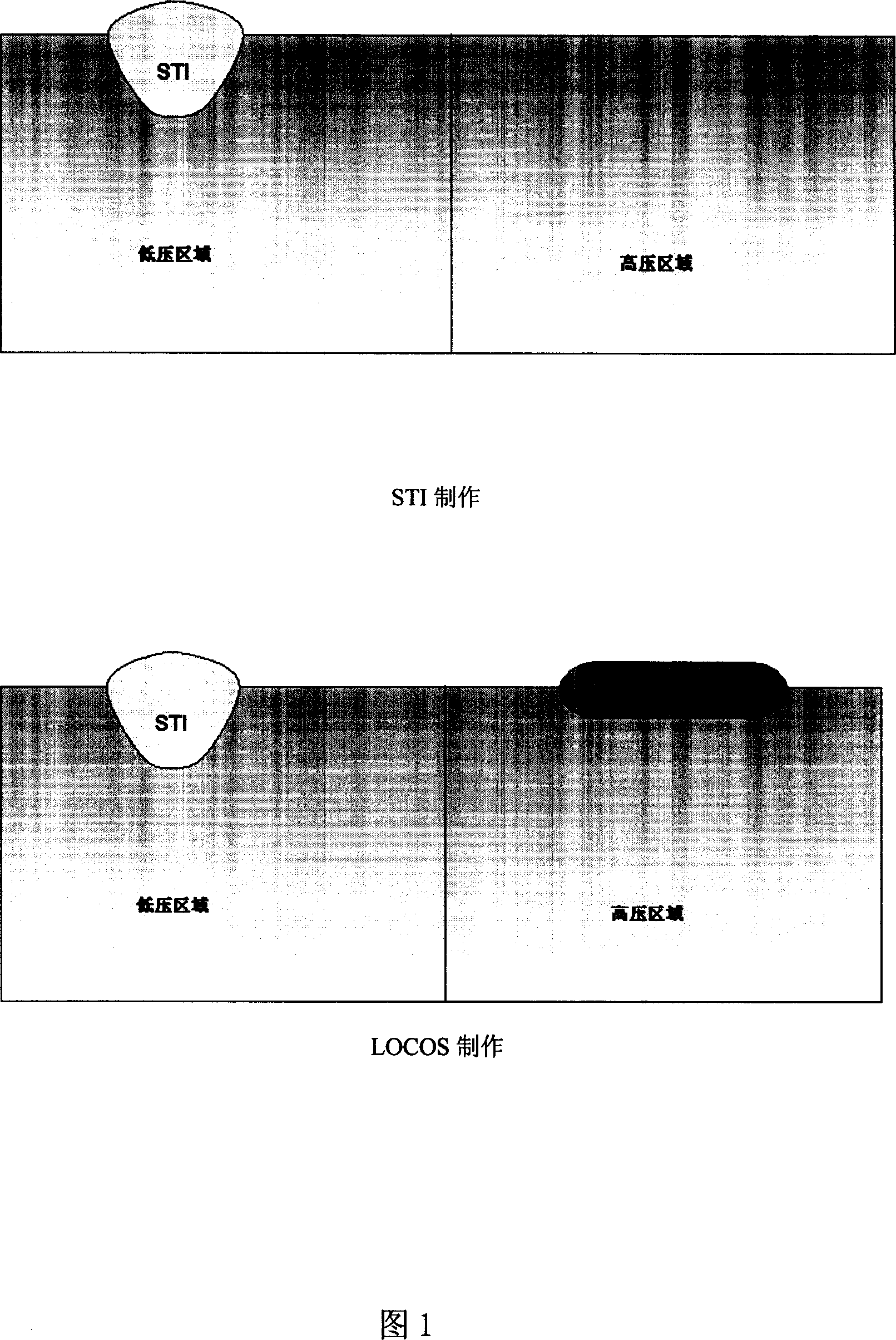
  • Device isolation structure used for high pressure manufacturing process and its manufacturing method
  • Device isolation structure used for high pressure manufacturing process and its manufacturing method
  • Device isolation structure used for high pressure manufacturing process and its manufacturing method

Examples


Embodiment Construction

[0019] In the existing high-voltage process technology, generally only one isolation structure among STI or LOCOS is selected for device isolation. The manufacturing process of the device isolation structure is generally placed in the initial stage of silicon wafer processing. The device isolation structure is firstly prepared on the silicon wafer through the standard STI or LOCOS process, and then the device structure and other subsequent processes are gradually completed.

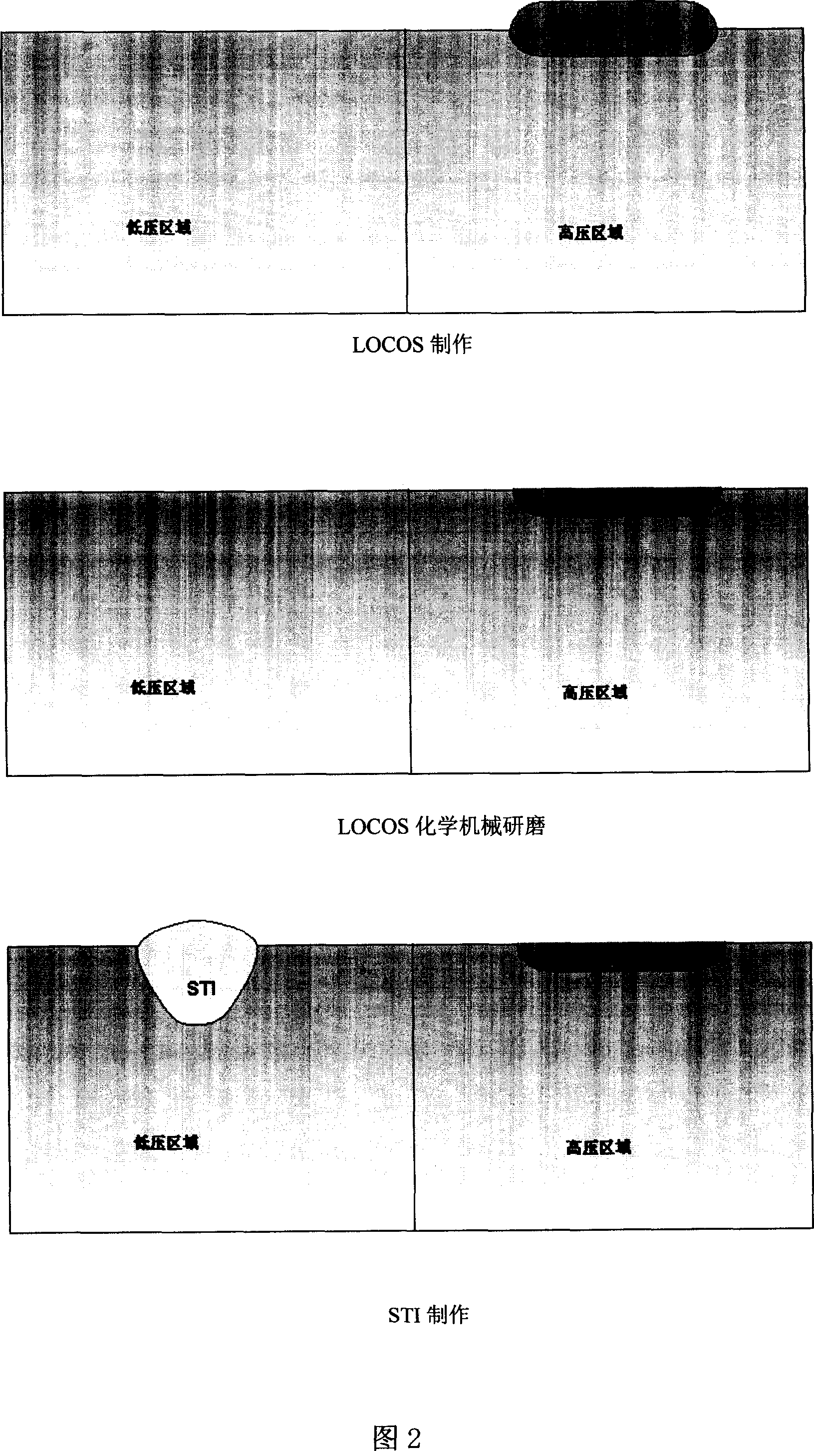
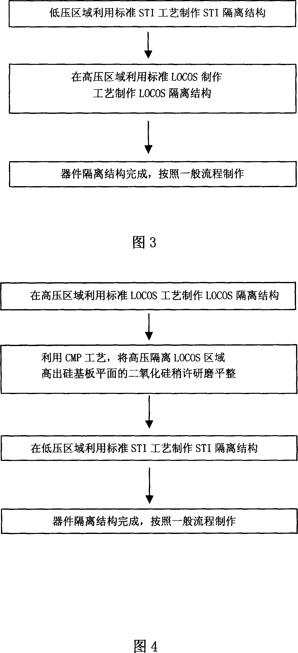
[0020] The present invention makes two isolation structures STI and LOCOS simultaneously in a high-pressure process. For device isolation in the low-voltage area, because the working voltage is not high, the isolation effect of the device is not high, so the STI isolation structure is adopted; for the device isolation in the high-voltage area, considering the high working voltage, in order to ensure good device isolation effect, Therefore, the LOCOS isolation structure is adopted. The manufacturing proce...


PUM


Abstract

The present invention discloses an element isolation structure for high voltage process, which comprises a semiconductor substrate provided with a low voltage zone and a high voltage zone, a STI isolation structure etched on the low voltage zone through light and a LOCOS isolation structure etched on the high voltage zone through light. The present invention also discloses technique and method to produce the element isolation structure, which minimizes module area occupied by the isolation structure based on the same isolation effect of elements.

Description

technical field [0001] The invention relates to a semiconductor device structure, in particular to a device structure for shallow trench isolation mixed local silicon oxidation isolation for high pressure process. The invention also relates to a manufacturing method of the device isolation structure. Background technique [0002] In the manufacturing process of modern semiconductor devices, shallow trench isolation (STI) and local oxide isolation of silicon (LOCOS) are two device isolation structures commonly used. LOCOS has a good isolation effect, but occupies a larger area than STI. With the continuous development of semiconductor device manufacturing technology, the device size is continuously reduced, and the requirements for the area occupied by the device isolation structure are strengthened. Due to its relatively small area, STI has become the mainstream device isolation structure used in advanced manufacturing processes. However, due to the characteristics of its...

Claims


Application Information

Patent Timeline
IPC IPC(8): H01L27/04H01L21/822H01L21/762
Inventor 钱文生陈晓波伍宏
Owner SHANGHAI HUA HONG NEC ELECTRONICS
Learn More