A process for large-scale production of CdTe/CdS thin film solar cells, without the use of CdCl2
A solar cell, large-scale technology, applied in the field of solar cells, which can solve the problems of low evaporation temperature, uneven deposition, danger, etc.
- Summary
- Abstract
- Description
- Claims
- Application Information
AI Technical Summary
Problems solved by technology
Method used
Image
Examples
Embodiment Construction
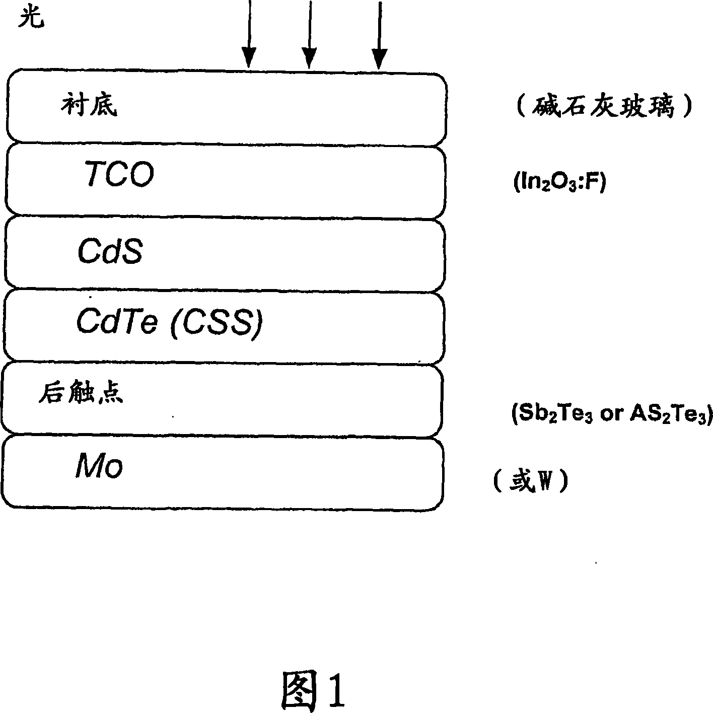
[0029] Referring to the figure, a CdTe / CdS solar cell produced by the method according to the present invention comprises five layers sequentially deposited on a transparent base layer or substrate, consisting of a 300-500 nm thick transparent conductive oxide (TCO) layer, on top of the TCO layer Deposited 80-200 nm thick CdS layer, 4-12 μm thick CdTe layer on top of the CdS layer and at least 100 nm thick SB 2 Te 3 layer and a 100nm thick Mo layer to form the rear contact layer. In particular, the transparent base substrate is composed of soda-lime glass, and the transparent conductive oxide doped with fluorine (In 2 o 3 :F).
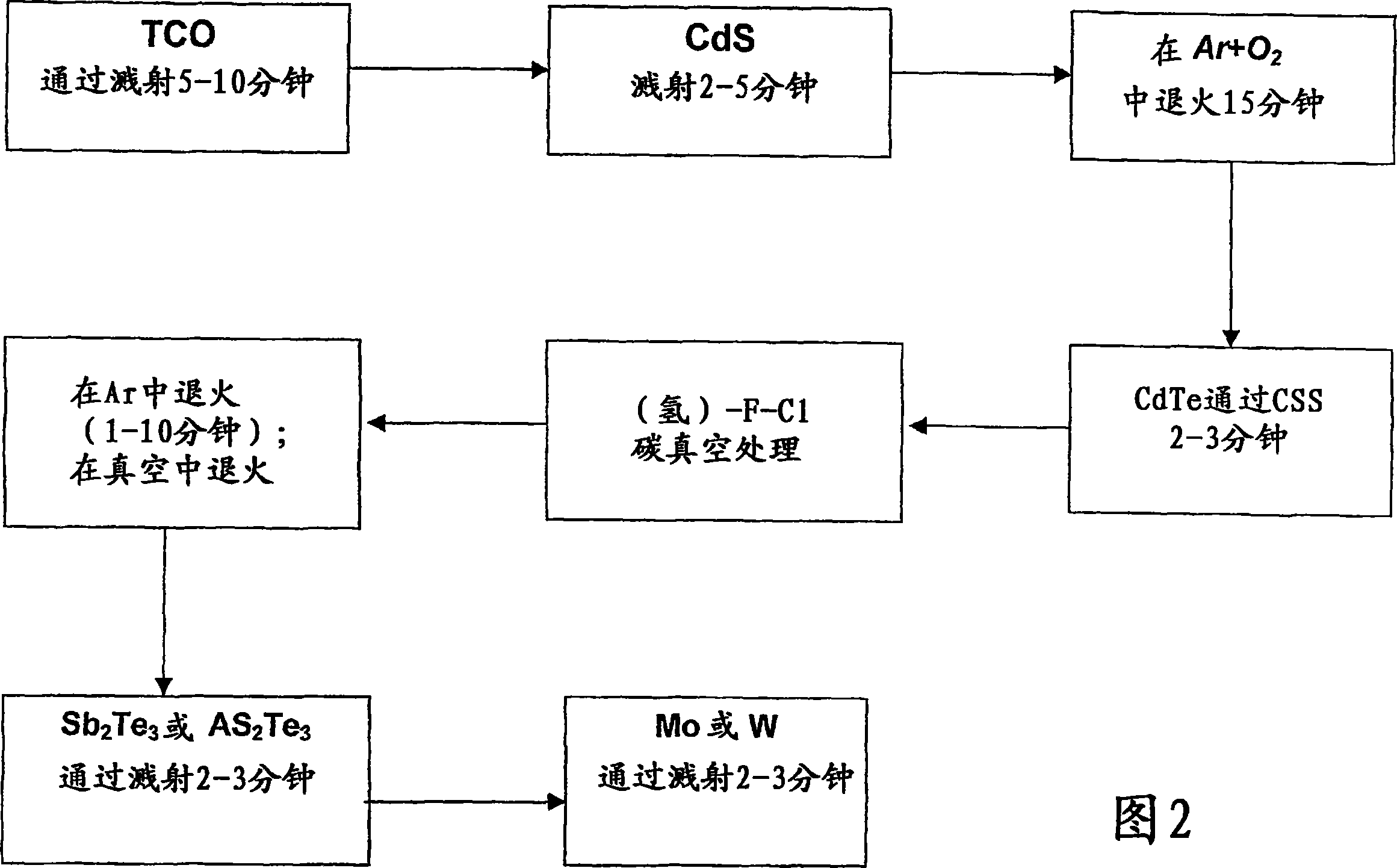
[0030] The TCO layer consists of fluorine-doped In during growth 2 o 3 composition. Different from ITO, In 2 o 3 The target does not form any needles. By introducing a gaseous fluoroalkyl compound, such as CHF, into the sputtering chamber 3 A small amount of fluorine and a mixture with an inert gas, such as Ar+H 2 A small amount of H in the ...
PUM
 Abstract
Description
Claims
Application Information


