Device for correcting input offset voltage
A technology of offset voltage and correction device, which is applied to the components of the amplification device, electrical components, amplifiers, etc., can solve the problems of high circuit cost, inability to increase the working bandwidth, and deterioration of operational amplifier characteristics, so as to achieve the goal of improving the application Effect
- Summary
- Abstract
- Description
- Claims
- Application Information
AI Technical Summary
Problems solved by technology
Method used
Image

Examples
Embodiment Construction
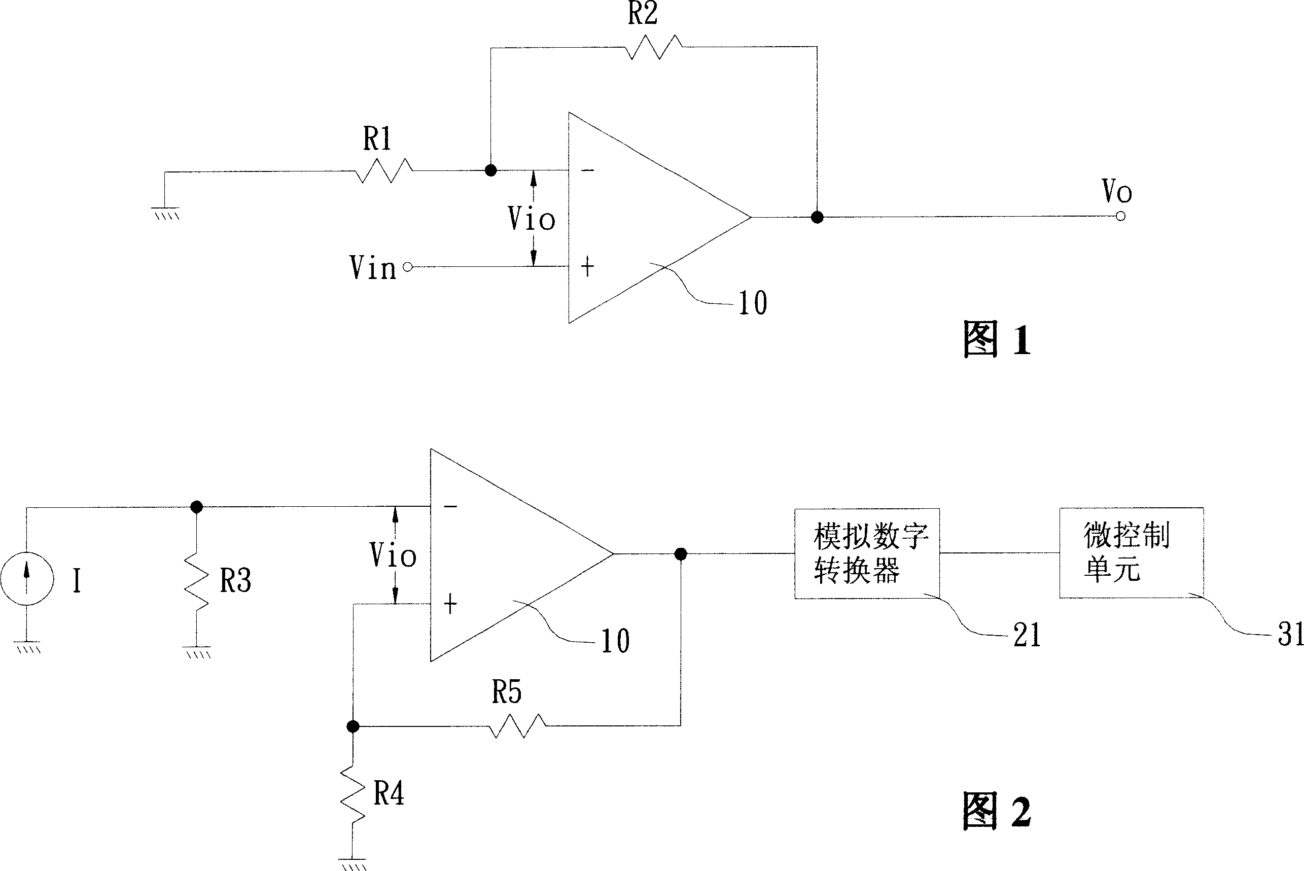
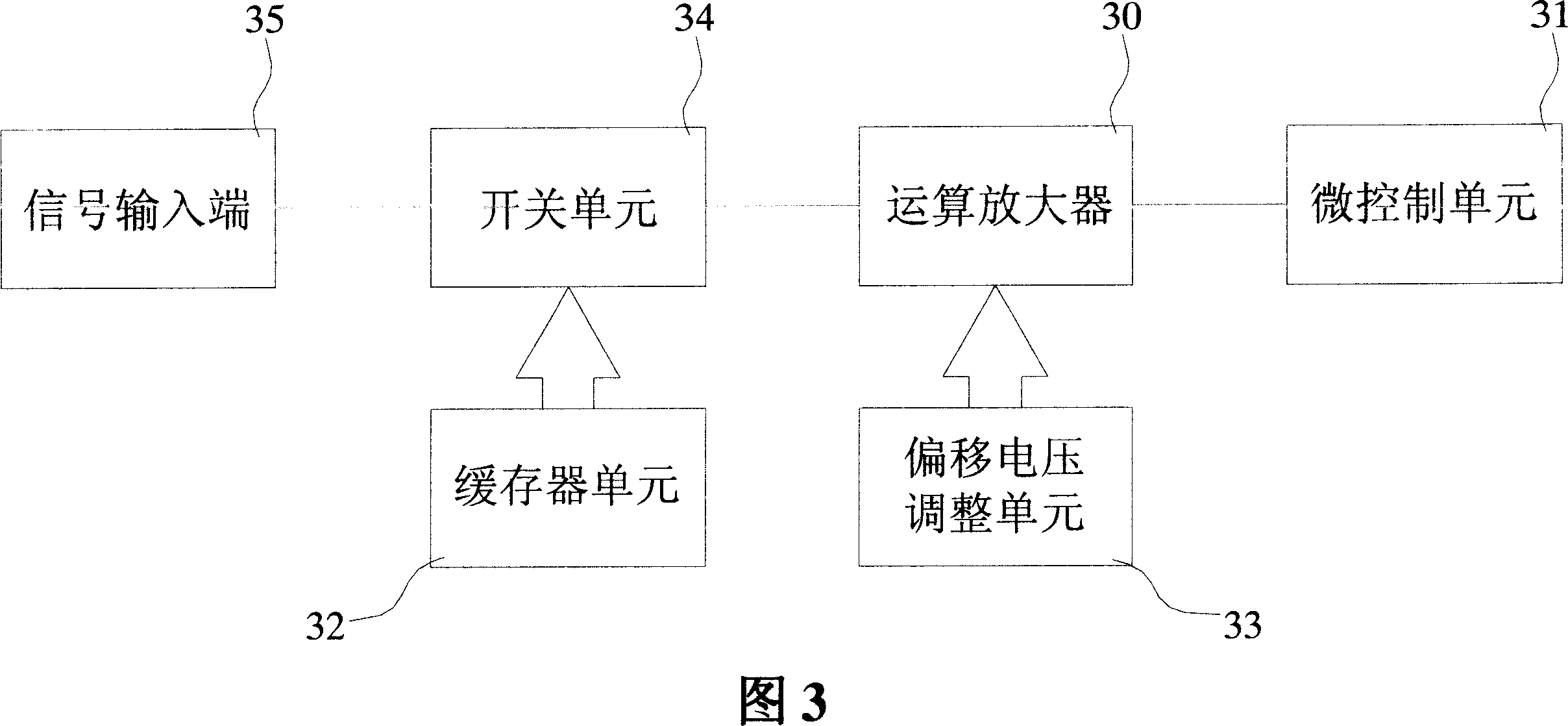
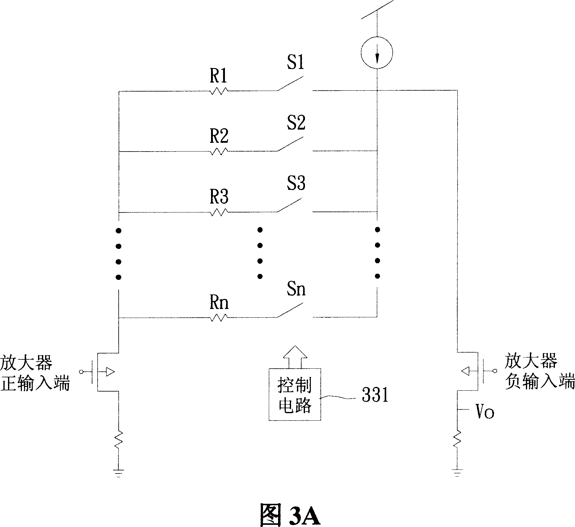
[0029] Please refer to FIG. 3 , which is a functional block diagram of the input offset voltage correction device of the present invention. The input offset voltage calibration device includes a register unit 32 , a micro control unit 31 , a switch unit 34 and an offset voltage adjustment unit 33 for adjusting the input offset voltage of the operational amplifier 30 . The signal input from the signal input terminal 35 is transmitted to the operational amplifier 30 through the switch unit 34 , and the signal is output to the micro control unit 31 by the operational amplifier 30 after being processed. In order to solve the impact caused by the input offset voltage of the operational amplifier 30, the microcontroller unit 31 will set the working mode switching signal in the register unit 32 to control the switching unit 34 to adjust the input offset voltage correction device in a normal working mode and Switch between an offset voltage correction mode. When the input offset volt...
PUM
 Abstract
Description
Claims
Application Information
 - R&D
- Intellectual Property
- Life Sciences
- Materials
- Tech Scout
- Unparalleled Data Quality
- Higher Quality Content
- 60% Fewer Hallucinations
Browse by: Latest US Patents, China's latest patents, Technical Efficacy Thesaurus, Application Domain, Technology Topic, Popular Technical Reports.
© 2025 PatSnap. All rights reserved.Legal|Privacy policy|Modern Slavery Act Transparency Statement|Sitemap|About US| Contact US: help@patsnap.com