Forming method for protecting image

A technology for protecting graphics and graphics, applied in the field of forming protection graphics, can solve the problems of low degree of freedom, increased sensitivity, and reduced degree of freedom of protective materials.

Active Publication Date: 2008-02-20
SANEI KAGAKU KK
View PDF1 Cites 14 Cited by
  • Summary
  • Abstract
  • Description
  • Claims
  • Application Information

AI Technical Summary

Problems solved by technology

[0007] However, solder resist materials are generally negative, and when direct exposure is performed, most of the patterned portion becomes the exposed portion, and the non-exposed portion is very small, so there is a concern that it will take a long time for direct exposure with laser light.
[0008] In addition, when the protective material is directly exposed to laser light, it is necessary to use a protective material with several times the sensitivity of the conventional one, so the protective material used is limited.
For example, when other components are mounted on a wiring board or a semiconductor substrate on which a protective film is patterned, the parts at the junction part on the wiring board need to have adhesiveness with resin or metal, but in this case, almost no A protective material that has both adhesion and sensitivity to laser light, but there is a concern that the degree of freedom in the selection of protective materials is low
As another example, when the protective film is made of a plating solution material, both chemical resistance and high sensitivity photosensitivity are required, and it is difficult to maintain chemical resistance and only increase the sensitivity
As a result, there is a concern that the degree of freedom in the choice of protective materials will decrease

Method used


Image

  • Forming method for protecting image
  • Forming method for protecting image
  • Forming method for protecting image

Examples


Embodiment 1

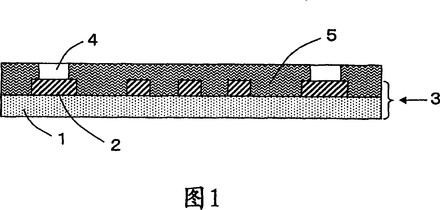
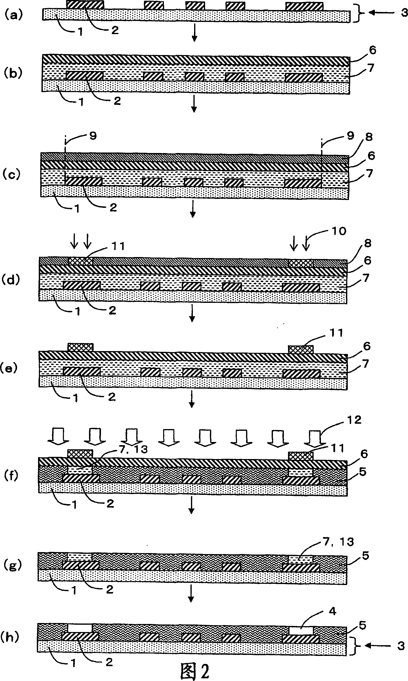
[0161] First, use a 150-mesh polyester screen to uniformly disperse the following ingredients 1) The resin composition was printed on a PE film 14 with a thickness of 100 μm, and dried at 80° C. for 15 minutes. In this way, the second photocurable protective film 8 is formed on the PE film 14 . Thereafter, a PET masking film 6 having a thickness of 25 μm was laminated on the upper surface of the second photocurable protective film 8 . In this way, a three-layer body composed of the PE film 14, the second photocurable protective film 8, and the PET masking film 6 was produced (see FIG. 6(a)).

[0162] On the other hand, the following combination composition 2) Alkali-developing type solder resist is screen-printed on the printed wiring board 3 on which the wiring pattern 2 has been formed, and the first photocurable protective film 7 is formed on the printed wiring board 3 (see FIG. 6(b) ).

[0163] Next, the above-mentioned three-layer body was laminated on the first photo...


PUM

PropertyMeasurementUnit
particle sizeaaaaaaaaaa
acid valueaaaaaaaaaa
particle sizeaaaaaaaaaa

Abstract

Production of a resist pattern involves applying first then second photohardenable resist films (F1, F2), sensitive to light in first and second wavelength regions (WL1, WL2) respectively, to a semiconductor chip or a circuit board, where film F2 blocks light of WLR1. Laser light in WL2 is applied through a screen onto part of F2 followed by applying a developer solution, to form a mask pattern. F1 is illuminated with light in WL1 through a membrane mask, and finally F1 is developed.

Description

[0001] technology area [0002] The present invention relates to a method for forming a resist pattern, and in particular to a resist pattern that can shorten exposure time and improve production efficiency when forming a pre-set solder resist when soldering on a printed wiring board. A formation method, and a formation method of a protective pattern that can increase the degree of freedom used in solder resist. Background technique [0003] In the manufacture of printed wiring boards, photosensitive materials are used as etching resist materials for circuit formation or solder resist materials for circuit protection. [0004] Conventionally, when pattern-exposing these protective materials, it is common to develop a construction method by irradiating ultraviolet light through a mask (hereinafter also referred to as a mask) formed with a light-shielding negative pattern such as glass or film. [0005] However, in the case of pattern exposure using a mask, it takes cost and ti...

Claims


Application Information

Patent Timeline
Patent Type & Authority Applications(China)
IPC IPC(8): G03F1/14G03F7/20G03F7/00H05K3/06G03F7/004G03F7/027G03F7/26G03F7/32H05K3/18H05K3/28
CPCH05K3/0082H05K2203/0551H05K2203/107H05K3/28G03F7/095H05K2203/066H05K2203/0577G03F7/038G03F7/0045G03F7/0047G03F7/0382H01L21/027H01L21/0271
Inventor 北村和宪佐藤清井上荣一
Owner SANEI KAGAKU KK
Why Eureka
Try Eureka