Surface light source apparatus, optical conductor used therefor and its manufacturing method

A technology of light guide body and surface light source, applied in the field of light guide body, can solve the problem of obvious uneven brightness

Inactive Publication Date: 2008-02-20
MITSUBISHI RAYON CO LTD
View PDF11 Cites 12 Cited by
  • Summary
  • Abstract
  • Description
  • Claims
  • Application Information

AI Technical Summary

Problems solved by technology

However, for the surface light source device using this light guide, it is often observed within the effective display range due to the size of the surface light source device, the number of point light sources such as LEDs, or the arrangement interval of point light sources. Obvious brightness unevenness caused by the overlapping of bright stripe-shaped brightness unevenness in the oblique direction of the light emitted by each point light source shown in Figure 76

Method used


Image

  • Surface light source apparatus, optical conductor used therefor and its manufacturing method
  • Surface light source apparatus, optical conductor used therefor and its manufacturing method
  • Surface light source apparatus, optical conductor used therefor and its manufacturing method

Examples


Embodiment 1~11、 comparative example 1~5

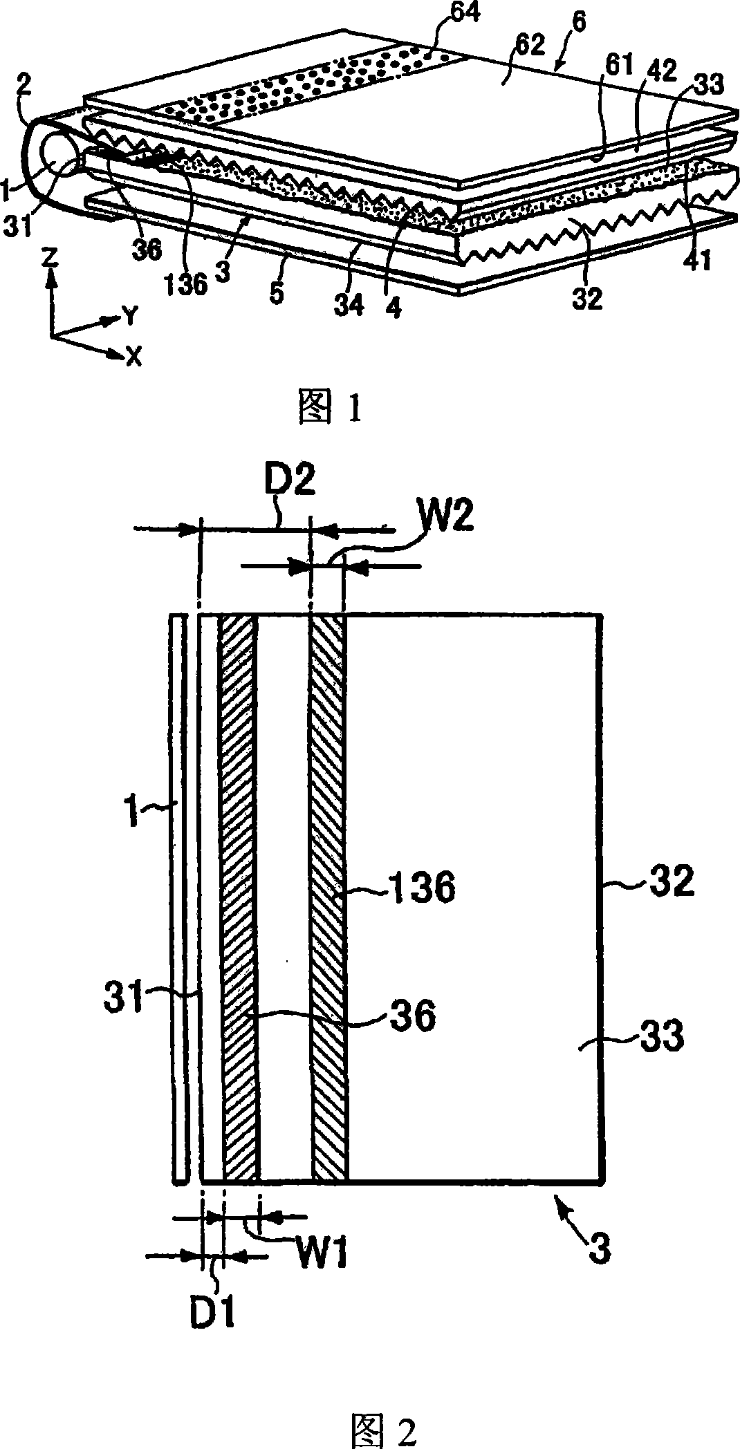
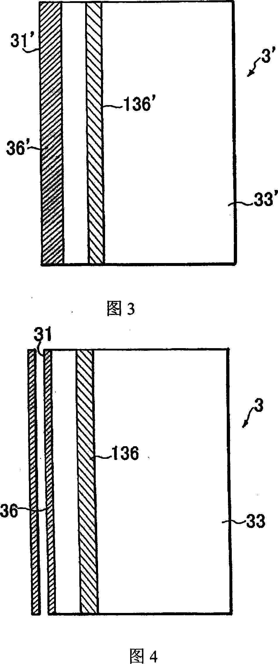
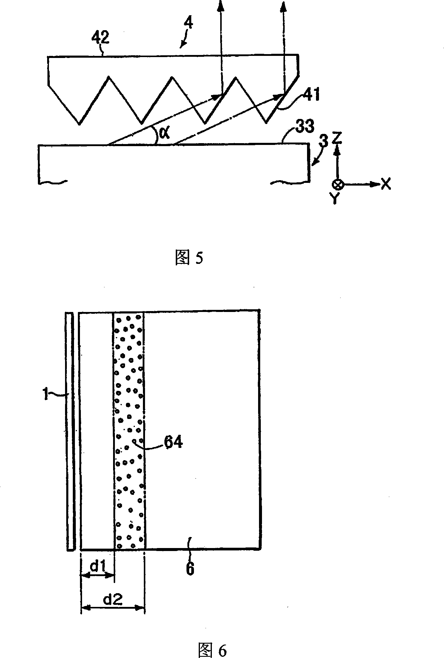
[0456] Using acrylic resin (ACRYPET (trade name) manufactured by Mitsubishi Rayon Co., Ltd.) by injection molding, a rectangular and wedge-shaped light guide material is produced. One side of the material is rough, and the other side is a prism corner. A prism column with 100 degrees, a top tip curvature radius of 15 μm, and a pitch of 50 μm. The prism column is a prism pattern continuously arranged parallel to the short side. The black ink described below was applied by screen printing to various widths (Examples 1 to 11, Comparative Examples 1 to 5) from the thicker long side on the rough surface of the light guide material on which the prism pattern was formed. A portion corresponding to the first light absorption band is formed. When the black ink was printed on a transparent acrylic plate with a thickness of 2 mm in the same manner as the visible light transmittance, the visible light transmittance of the ultraviolet curable black ink was 30%. Simultaneously, a second li...

Embodiment 8

[0472] Embodiment 8——W1=300 μm, D2=900 μm, W2=300 μm

Embodiment 9

[0473] Embodiment 9——W1=300 μm, D2=900 μm, W2=150 μm


PUM

PropertyMeasurementUnit
widthaaaaaaaaaa
widthaaaaaaaaaa
diameteraaaaaaaaaa

Abstract

Even when using a light source reflector having a strong direct reflection tendency in an edge light type planar light source device, the light coming from the primary light source into the light incident end surface and introduced into the light guide is not shielded, the entire luminance lowering is not caused, generation of dark-lines is not caused by shielding of the light to be guided, generation of the bright-lines in the vicinity of light incident end surface is prevented for a long period of time, and generation of sudden local luminance change is prevented. In the light guide (3) using a primary light source (1) in combination with a light source reflector (2), a first light absorption band (36) and a second light absorption band (136) extending along the light incident end surface (31) are arranged in parallel on the light emitting surface (33). The first light absorption band (36) has a width of 50 [mu]m to 800 [mu]m. The first light absorption band (36) has the side edge in the vicinity of the light incident end surface (31) is at a distance of 300 [mu]m or less from the light incident end surface. The second light absorption band (136) has the side edge in the vicinity of the light incident end surface (31) is at a distance of 500 [mu]m to 3000 [mu]m from the light incident end surface.

Description

technical field [0001] The present invention relates to an edge-illuminated surface light source device and a light guide used therefor, and specifically relates to trying to reduce the number of striped bright lines along the light incident end surface near the light incident end surface of the light guide opposite to the primary light source. A surface light source device and its dedicated light guide body and its manufacturing method for the phenomenon of non-uniform brightness distribution observed in the form of dark lines and / or dark lines. The surface light source device of the present invention is more suitable for the backlight of liquid crystal display devices, for example. [0002] In addition, the present invention particularly relates to a surface light source device that aims at miniaturization and reduction in power consumption. The surface light source device of the present invention is more suitable for use as a surface light source device of a relatively sma...

Claims


Application Information

Patent Timeline
Patent Type & Authority Applications(China)
IPC IPC(8): F21V8/00G02B6/00G02F1/13357F21Y103/00G02F1/1335
Inventor 山下友义林健太郎川岛伯夫
Owner MITSUBISHI RAYON CO LTD
Why Eureka
Try Eureka