Vertical gallium nitride-based light emitting diode and method of manufacturing the same

A light-emitting diode, gallium nitride-based technology, applied in electrical components, circuits, semiconductor devices, etc., can solve problems such as reducing the reliability of LEDs

Active Publication Date: 2008-02-27
SAMSUNG ELECTRONICS CO LTD
View PDF2 Cites 33 Cited by
  • Summary
  • Abstract
  • Description
  • Claims
  • Application Information

AI Technical Summary

Problems solved by technology

Therefore, a piezoelectric effect is generated, which will reduce the reliability of the LED

Method used


Image

  • Vertical gallium nitride-based light emitting diode and method of manufacturing the same
  • Vertical gallium nitride-based light emitting diode and method of manufacturing the same
  • Vertical gallium nitride-based light emitting diode and method of manufacturing the same

Examples


no. 1 Embodiment approach

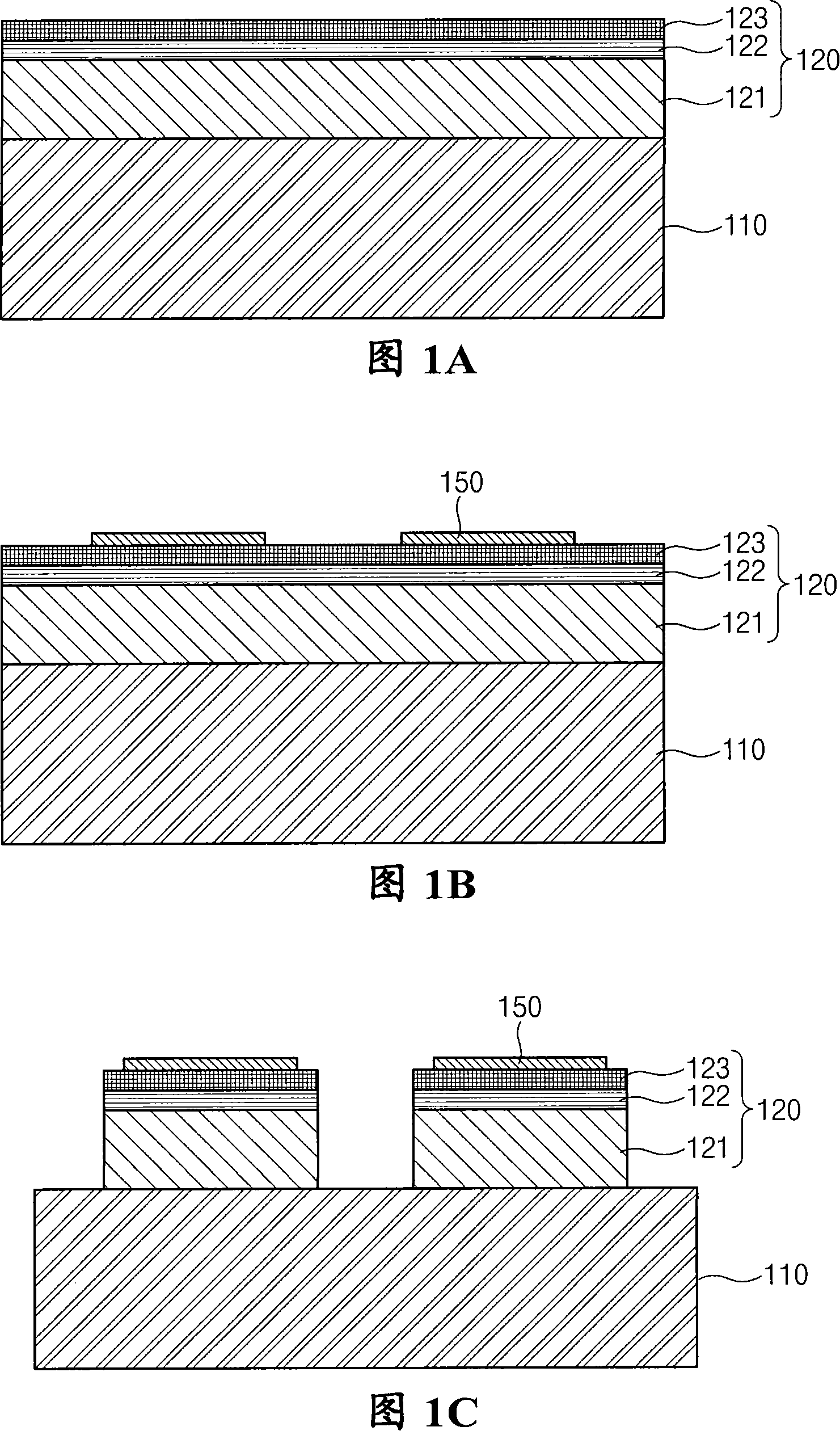
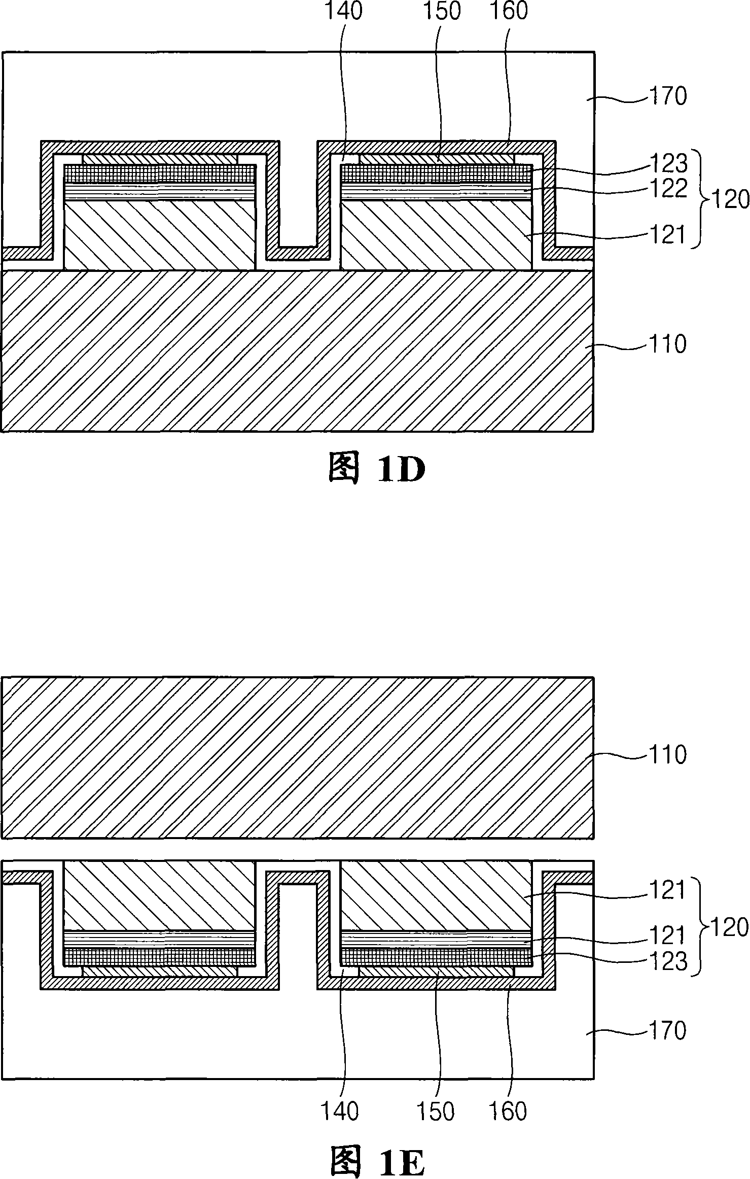
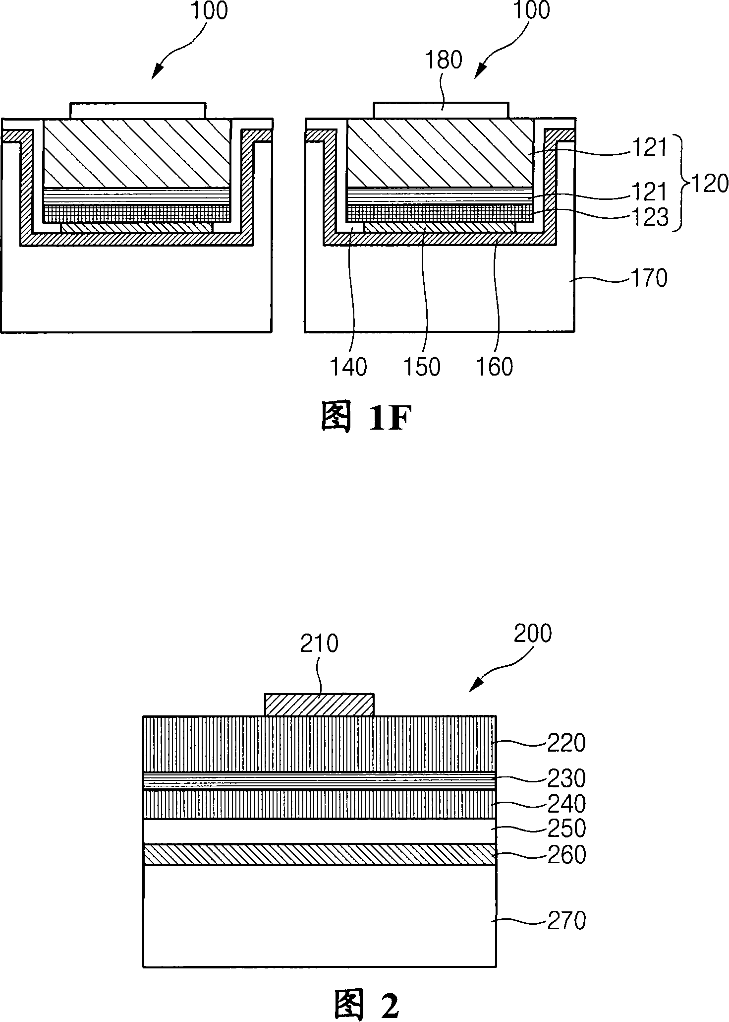
[0058] Referring to FIGS. 3 and 4A to 4M , a vertical GaN-based LED and a method of manufacturing the same according to a first embodiment will be described in detail.

[0059] 3 is a cross-sectional view showing a vertical GaN-based LED structure according to a first embodiment of the present invention. 4A to 4M are cross-sectional views sequentially showing a vertical GaN-based LED manufacturing method according to a first embodiment of the present invention.

[0060] As shown in FIG. 4A, a light emitting structure 320 is formed on a substrate 310, and the light emitting structure 320 is composed of a GaN-based semiconductor layer. In the light emitting structure 320, an n-type GaN-based semiconductor layer 321, an active layer (active layer) 322 composed of a GaN / InGaN layer having a multi-quantum well structure, and a p-type GaN-based semiconductor layer 323 are sequentially stacked. .

[0061] Preferably, the substrate 310 is formed of a transparent material including s...

no. 2 Embodiment approach

[0090]

[0091] A vertical GaN-based LED according to a second embodiment of the present invention will be described in detail with reference to FIGS. 5 to 8 .

[0092] 5 is a cross-sectional view showing a vertical GaN-based LED according to a second embodiment of the present invention. 6 to 8 are plan views illustrating shapes of reflective electrodes according to the present invention.

[0093] As shown in FIG. 5, the vertical GaN-based LED 400 according to the second embodiment has an n-electrode 410 at its uppermost portion.

[0094] Under the n-electrode 410, an n-type GaN-based semiconductor layer 420 is formed. More specifically, the n-type GaN-based semiconductor layer 420 may be formed of a GaN layer or a GaN / AlGaN layer doped with n-type impurities.

[0095] In order to enhance the current spreading effect, a transparent electrode (not shown) is further formed between the n-electrode 410 and the n-type GaN-based semiconductor layer 420 .

[0096] Under the n-ty...

no. 3 Embodiment approach

[0117]

[0118] Next, a third specific embodiment of the present invention will be described with reference to FIGS. 10 to 12 . Wherein, the description of the same parts as those of the second specific embodiment is omitted.

[0119] 10 to 12 are cross-sectional views illustrating the structure of a vertical GaN-based LED according to a third embodiment of the present invention.

[0120]As shown in FIGS. 10 to 12 , the vertical GaN-based LED according to the third embodiment has substantially the same configuration as the vertical GaN-based LED according to the second embodiment. However, the vertical GaN-based LED according to the third embodiment is different from the vertical GaN-based LED according to the second embodiment in that the blocking layer 455 is formed of an insulating film so that a part of the reflective electrode is formed to be exposed. outside. The insulating film can be made of oxide-based or nitride-based materials such as SiO 2 、Al 2 o 3 、TiO 2 ...


PUM


Abstract

A vertical gallium nitride-based light emitting diode and a manufacturing method thereof are provided to prevent junction leakage and a short circuit by preventing atoms composing a metal seed layer from penetrating into an active layer. A light emission structure(120) comprising an n-type GaN-based semiconductor layer(121), an active layer, and a p-type GaN-based semiconductor layer(123) is formed on a substrate, and then is etched to divide the light emission structure into units of LED(100). A p-electrode(150) is formed on each of the divided light emission structures, and a non-conductive material is filled between the divided light emission structures. A metal seed layer(160) is formed on the structure, and a first plated layer(170a) is formed on the metal seed layer excluding a region between the light emission structures. A second plated layer(170b) is formed on the metal seed layer between the first plated layers. The substrate is separated from the light emission structures, and then the non-conductive material is removed between the light emission structures exposed by separating the substrate. An n-electrode(180) is formed on the n-type GaN-based semiconductor layer, and then portions of the metal seed layer and the second plated layer are removed between the light emission structures.

Description

[0001] Cross References to Related Applications [0002] This application claims Korean Patent Application No. 10-2006-0079703 filed with the Korean Intellectual Property Office on Aug. 23, 2006 and Korean Patent Application No. 10-2007-0017519 filed with the Korean Intellectual Property Office on Feb. 21, 2007 priority, the contents of which are hereby incorporated by reference. technical field [0003] The present invention relates to a vertical gallium nitride-based light emitting diode (hereinafter, referred to as a "vertical GaN-based LED") and a method of manufacturing the same, which can enhance the reliability of the LED. Background technique [0004] Typically, nitride-based semiconductor LEDs are grown on sapphire substrates (substrates), but such sapphire substrates are rigid non-conductors and have poor thermal conductivity. Therefore, there is a limit in reducing the manufacturing cost by reducing the size of the nitride-based semiconductor LED or by improving ...

Claims


Application Information

Patent Timeline
Patent Type & Authority Applications(China)
IPC IPC(8): H01L33/00H01L33/06H01L33/10H01L33/14H01L33/22H01L33/32H01L33/38H01L33/40
Inventor 李守烈吴邦元白斗高张泰盛禹钟均崔锡范尹相皓金东佑吕寅泰
Owner SAMSUNG ELECTRONICS CO LTD
Why Eureka
Try Eureka