Method for sticking module group substrates with driver circuit and equipment thereof

A driving circuit and liquid crystal module technology, which is applied in nonlinear optics, instruments, optics, etc., can solve problems such as substrate warping, low product yield, and driving circuit bonding dislocation, so as to reduce maneuvering space, improve yield, Avoid the effect of adhesive misalignment

Inactive Publication Date: 2008-03-12
AU OPTRONICS (SUZHOU) CORP LTD
View PDF0 Cites 8 Cited by
  • Summary
  • Abstract
  • Description
  • Claims
  • Application Information

AI Technical Summary

Problems solved by technology

Its purpose is to solve the technical problems that the existing large-size LCD module bonding equipment causes seri

Method used


Image

  • Method for sticking module group substrates with driver circuit and equipment thereof
  • Method for sticking module group substrates with driver circuit and equipment thereof
  • Method for sticking module group substrates with driver circuit and equipment thereof

Examples


Embodiment 1

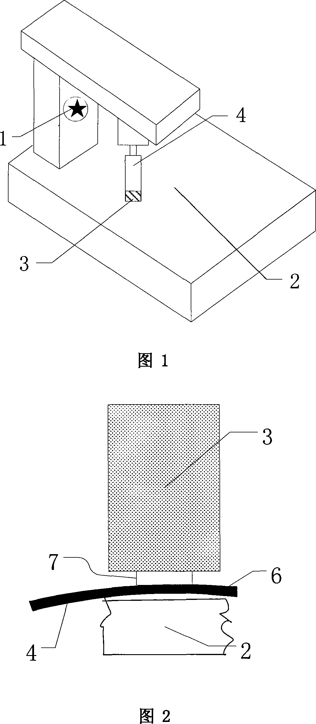
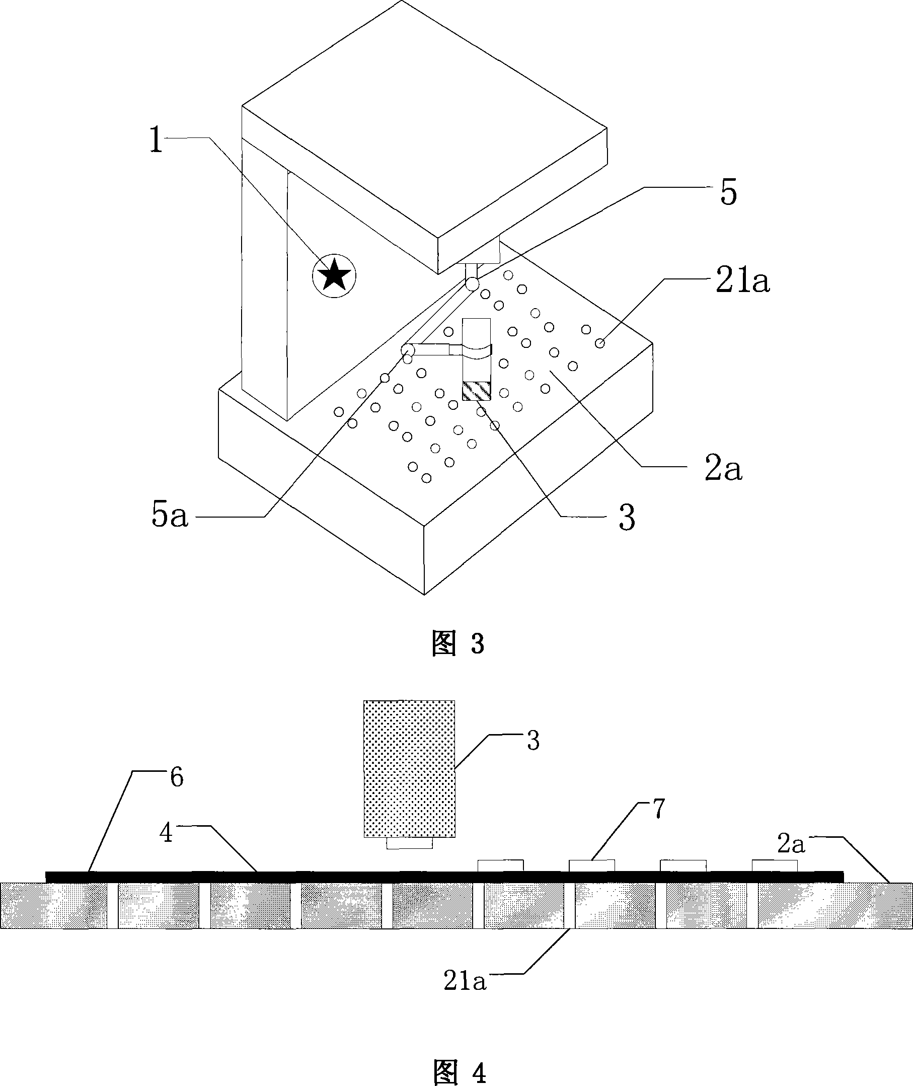
[0033] 3 to 5 are a schematic structural diagram and a working schematic diagram of a bonding apparatus according to a preferred embodiment of the present invention. As can be seen from FIG. 3 , the bonding apparatus of this embodiment includes a digital program-controlled unit 1 , a support table 2 a , a thermal pressing head 3 and a driving mechanism 5 thereof. The support table 2a is provided with a plurality of vacuum suction holes 21a; the digital program control unit 1 is used to drive the drive mechanism 5 to control the action of the thermal head 3 . As shown in FIG. 4 , when entering the LCD module segment process, the LCD module substrate 6 is placed on the support table 2a for vacuum adsorption, and the LCD module substrate 6 can be firmly adsorbed on the vacuum suction hole 21a through the vacuum suction hole 21a. The support table 2a is kept in a flat and stable state; the digital program control unit 1 in the machine equipment drives the driving mechanism 5 to tr...

Embodiment 2

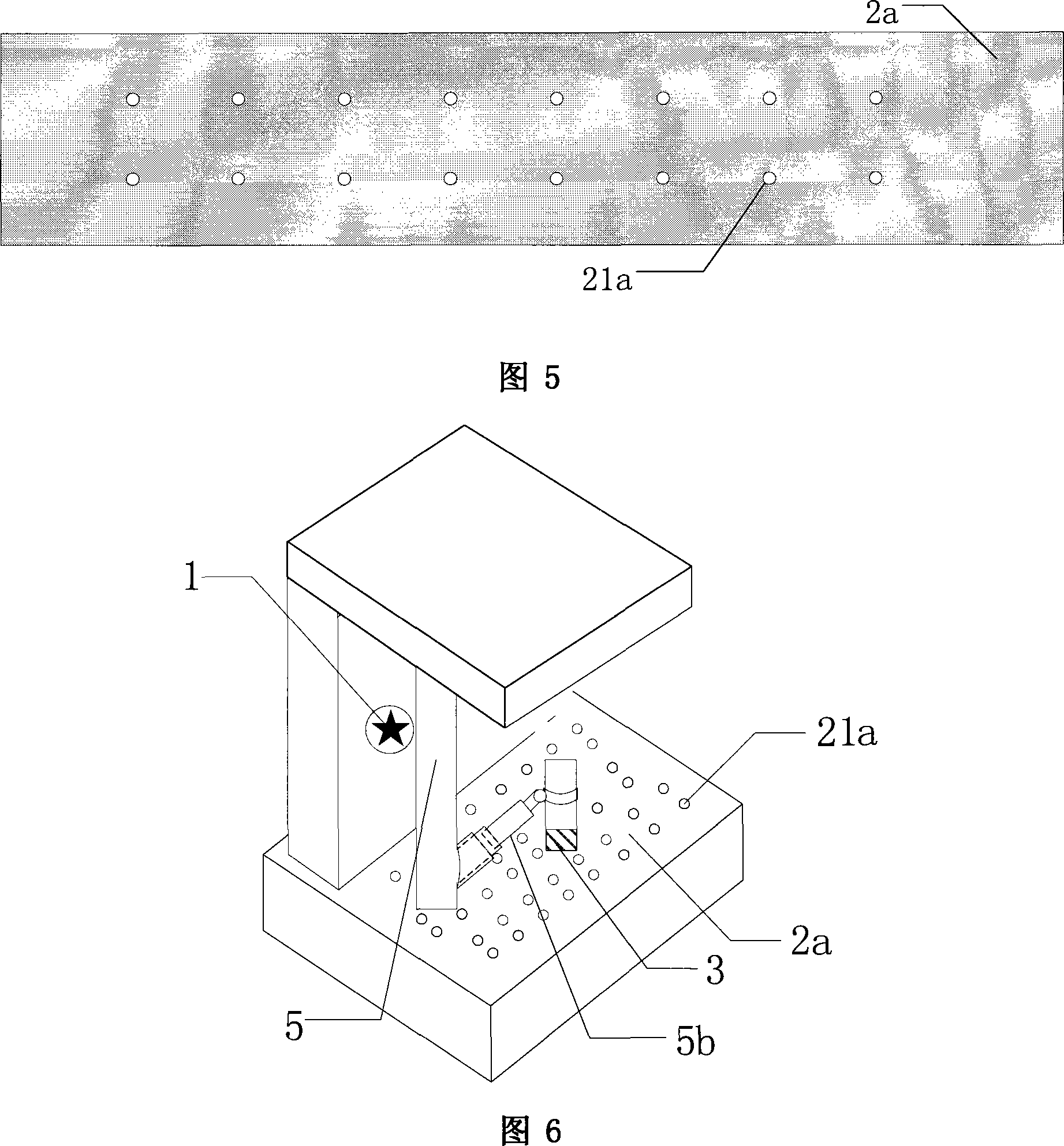
[0035] FIG. 6 is a schematic structural diagram and a working schematic diagram of a bonding apparatus according to another embodiment of the present invention. It can be seen from the figure that the processing equipment of this embodiment also includes a digital program control unit 1 , a support table 2 b , a thermal press head 3 and its driving mechanism 5 . The difference is that the driving mechanism 5 in this embodiment adopts a telescopic straight tube type lateral displacement member 5b.

[0036] The placement of the liquid crystal module substrate 6 on the support table 2a is as described in the first embodiment. In particular, the digital program control unit 1 drives and controls the telescopic straight-tube lateral displacement mechanism 5b of the thermal head 3 according to a specific program. Start to extend step by step along the liquid crystal module substrate 6, and drive the thermal head 3 at the matching position to press the driving circuit 7 and the liqui...


PUM


Abstract

The present invention discloses a method of gluing a liquid crystal module substrate with a drive circuit and a device. Wherein, the method includes steps below: Fixing a liquid crystal module substrate onto a supporting table to absorb the liquid crystal module substrate through vacuum; driving a thermal compression head to move horizontally to press the drive circuit with the substrate one by one. In addition, the gluing device comprises a digital program control unit, a supporting table, a thermal compression head and a drive mechanism, of which the thermal compression head is driven by the drive mechanism to shift horizontally. Vacuum intakes are arranged on the supporting table. The gluing method and the device of the present invention can not only avoid aberration resulting from the substrate deformation due to larger liquid crystal module substrate during pressing and improve rate of quality products but also reduce revolving space of the liquid crystal module substrate in the device and shrink overall device size.

Description

technical field [0001] The present invention relates to the manufacture of liquid crystal panel (LCD), in particular to a method and equipment for bonding and processing a liquid crystal module substrate and a driving circuit in the LCD manufacturing process. Background technique [0002] With the continuous advancement of human science and technology, display technology has also made a qualitative leap in a short period of time. The advent of liquid crystal displays (LCDs) has gradually replaced the traditional cathode ray tube displays (CRTs), marking that display technology has entered a new era. the height of. As far as LCD is concerned, the bright and dark effects are obtained through external voltage control and the electro-optic effect of liquid crystal molecules, thereby generating colorful colors and images to achieve the purpose of displaying images. In particular, the Thin Film Transistor Liquid Crystal Display (TFT-LCD) invented in 1960 has been successfully com...

Claims


Application Information

Patent Timeline
IPC IPC(8): G02F1/13G02F1/133G02F1/1345
Inventor 付博陆海江孙涛
Owner AU OPTRONICS (SUZHOU) CORP LTD
Why Eureka
Try Eureka