
Photoresist composition and method of forming a resist pattern

A photoresist material and integrated circuit technology, which is applied to photosensitive materials, circuits, and patterned surface photoengraving processes for optomechanical equipment, etc., can solve problems such as pattern collapse, and achieve the effect of reducing collapse and strengthening adhesion.

Active Publication Date: 2008-03-12
TAIWAN SEMICON MFG CO LTD
View PDF0 Cites 8 Cited by
  • Summary
  • Abstract
  • Description
  • Claims
  • Application Information

AI Technical Summary

Problems solved by technology

However, thick photoresist layers suffer from pattern collapse

Method used


Image

  • Photoresist composition and method of forming a resist pattern
  • Photoresist composition and method of forming a resist pattern
  • Photoresist composition and method of forming a resist pattern

Examples


Embodiment Construction

[0056] It can be understood that the following disclosure provides different embodiments or examples to implement various embodiments with different features. The specific examples of parts and arrangements described below simplify the invention. Of course, the above are only examples and are not intended to limit the present invention. For example, forming the first feature on or above the second feature may include several embodiments in which the first feature and the second feature form direct contact in the following description, and may also include additional features formed on the first feature. Several embodiments between the feature and the second feature, so that the first feature and the second feature are not in direct contact. In addition, the content of the disclosure will repeatedly refer to figure numbers and / or texts in different examples. The above repetition is for the purpose of simplification and clarification, and is not used to limit the relationship betwee...


PUM

PropertyMeasurementUnit
sizeaaaaaaaaaa
molecular weightaaaaaaaaaa
thicknessaaaaaaaaaa

Abstract

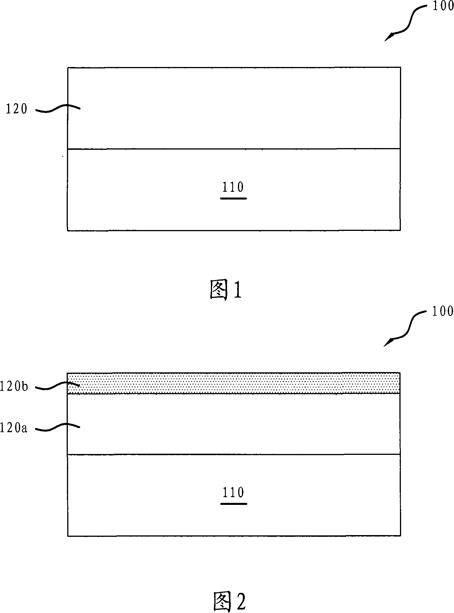
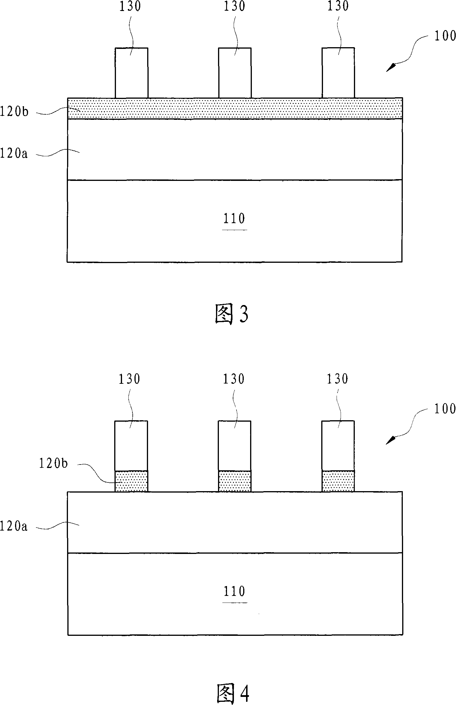
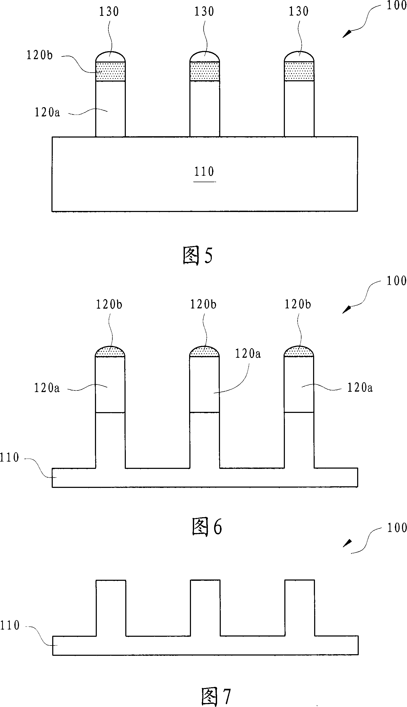
The invention related to photoresist material for microimage pattern and method of forming integrated circuit pattern, the photoresist material includes a first material, and a second material dispersed in the first material. The second material is capable of diffusing to a top surface of the photoresist material, and has an etch rate different from that of the first material. The forming method of integrated circuit pattern includes at least: a lower layer formed on a substrate; a patterning photoresist layer formed on the lower layer; a top part using the patterning photoresist layer to etch the lower part; and a main part using the top part to etch the lower part.

Description

Technical field [0001] The invention relates to a photoresist material and a method for forming an integrated circuit pattern, in particular to a photoresist material for lithographic patterning and a method for forming an integrated circuit pattern to avoid the collapse of the photoresist. Background technique [0002] Semiconductor technology continues to develop toward smaller feature sizes, with sizes below 65 nanometers and 45 nanometers. The patterned photoresist layer used to produce the above-mentioned minute feature sizes generally has a high aspect ratio (aspectratio). For various reasons, maintaining a predetermined critical dimension (CD) becomes very difficult. For example, in order to maintain high etching resistance, a thick photoresist layer is usually used. However, the photoresist layer with a large thickness will encounter the problem of pattern collapse. Summary of the invention [0003] The purpose of the present invention is to overcome the shortcomings of ...

Claims


Application Information

Patent Timeline
Patent Type & Authority Applications(China)
IPC IPC(8): G03F7/075G03F7/004G03F7/00H01L21/027
CPCG03F7/094G03F7/091G03F7/0757G03F7/0047G03F7/11
Inventor 张庆裕
Owner TAIWAN SEMICON MFG CO LTD
Learn More