Array substrate, display panel and display device

A technology for array substrates and display panels, applied in semiconductor devices, electrical components, circuits, etc., can solve problems affecting the performance of OLED devices, affecting product work stability, and anode edge collapse, so as to improve work stability and prevent work stability Sexual impact, effect of reducing collapse

Active Publication Date: 2017-08-18
BOE TECH GRP CO LTD
View PDF4 Cites 11 Cited by
  • Summary
  • Abstract
  • Description
  • Claims
  • Application Information

AI Technical Summary

Problems solved by technology

When using the plasma vapor deposition process to prepare the inorganic pixel defining layer, the substances or gases in the preparation process will chemically react with the etching solution remaining on the planarization layer, resulting in holes in the planarization layer, causing the edge of the anode to collapse, and then affecting the performance of the OLED device.
[0004] In summary, the preparation process of the pixel defining layer in the prior art is easy to cause damage to the planarization layer, causing the edge of the anode to collapse and affecting the stability of the product.

Method used


Image

  • Array substrate, display panel and display device
  • Array substrate, display panel and display device
  • Array substrate, display panel and display device

Examples


Embodiment Construction

[0023] Embodiments of the present application provide an array substrate, a display panel, and a display device, which are used to reduce damage to the substrate during the preparation of the pixel defining layer, prevent the edge of the electrode layer from collapsing, and improve the working stability of the product.

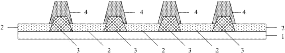
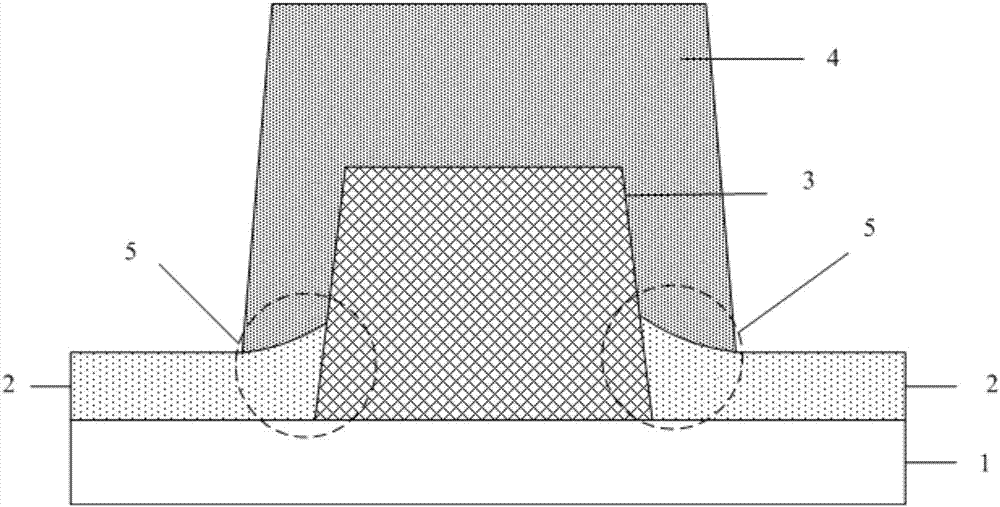
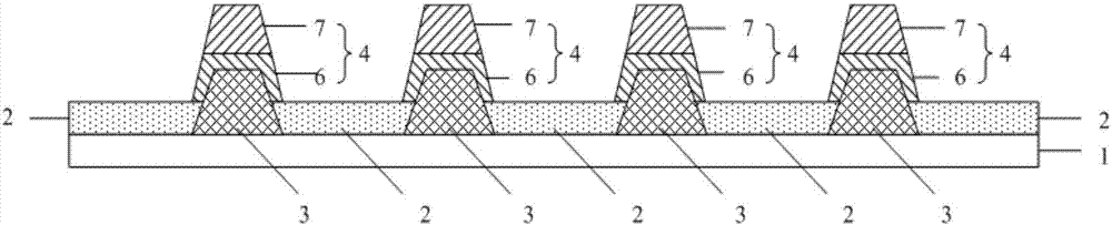
[0024] An array substrate provided in an embodiment of the present application, such as figure 1 As shown, the array substrate includes: a substrate 1, an electrode layer 2 disposed in an array on the substrate 1, a pad layer 3 located on the substrate 1 and spaced apart from the electrode layer 2 , and a pixel defining layer 4 located on the pad layer 3, the electrode layer is in contact with the pad layer.

[0025] In the array substrate provided in the embodiment of the present application, since the pad layer is located on the substrate, and the pixel defining layer is located on the pad layer, that is, a pad layer is provided between the pixel defining la...


PUM


Abstract

The invention discloses an array substrate, a display panel and a display device, which are used for reducing damage to a substrate during the fabrication process of a pixel defining layer and preventing an edge of an electrode layer from being collapsed so as to further improve the working stability of a product. The embodiment of the invention provides the array substrate. The array substrate comprises a substrate, electrode layers, block-up layers and pixel defining layers, wherein electrode layers are arranged on the substrate and are arranged in an array way, the block-up layers are arranged on the substrate and are isolated with the electrode layers at intervals, the pixel defining layers are arranged on the block-up layers, and the electrode layers are in contact with the block-up layers.

Description

technical field [0001] The present application relates to the field of display technology, and in particular to an array substrate, a display panel and a display device. Background technique [0002] Organic electroluminescent displays have the advantages of self-luminescence, fast response, wide viewing angle, high brightness, bright colors, light and thin, etc. Organic electroluminescent display technology has become an important display technology. [0003] For Organic Light Emitting Diode (OLED) or Polymer Light Emitting Diode (PLED) organic electroluminescent devices, there are two methods of forming organic thin films: vacuum evaporation and solution process. The vacuum evaporation method is suitable for small organic molecules. Its characteristics The formation of organic films does not require solvents, and the film thickness is uniform, but the equipment investment is large, the material utilization rate is low, and it is not suitable for the production of large-sca...

Claims


Application Information

Patent Timeline
Patent Type & Authority Applications(China)
IPC IPC(8): H01L27/32
CPCH10K59/122
Inventor 侯文军刘则
Owner BOE TECH GRP CO LTD
Why Eureka
Try Eureka