Making method for low on-resistance power VDMOS transistor

A technology of low on-resistance and manufacturing method, which is applied in the manufacture of low on-resistance power MOS transistors and the manufacture of low on-resistance power VDMOS transistors. R3 and other issues

Active Publication Date: 2008-03-26
NO 24 RES INST OF CETC
View PDF2 Cites 16 Cited by
  • Summary
  • Abstract
  • Description
  • Claims
  • Application Information

AI Technical Summary

Problems solved by technology

Due to the increase of the concentration of the whole layer, the depletion layer of the VDMOS transistor facing the P well and the drain

Method used


Image

  • Making method for low on-resistance power VDMOS transistor
  • Making method for low on-resistance power VDMOS transistor
  • Making method for low on-resistance power VDMOS transistor

Examples


Embodiment Construction

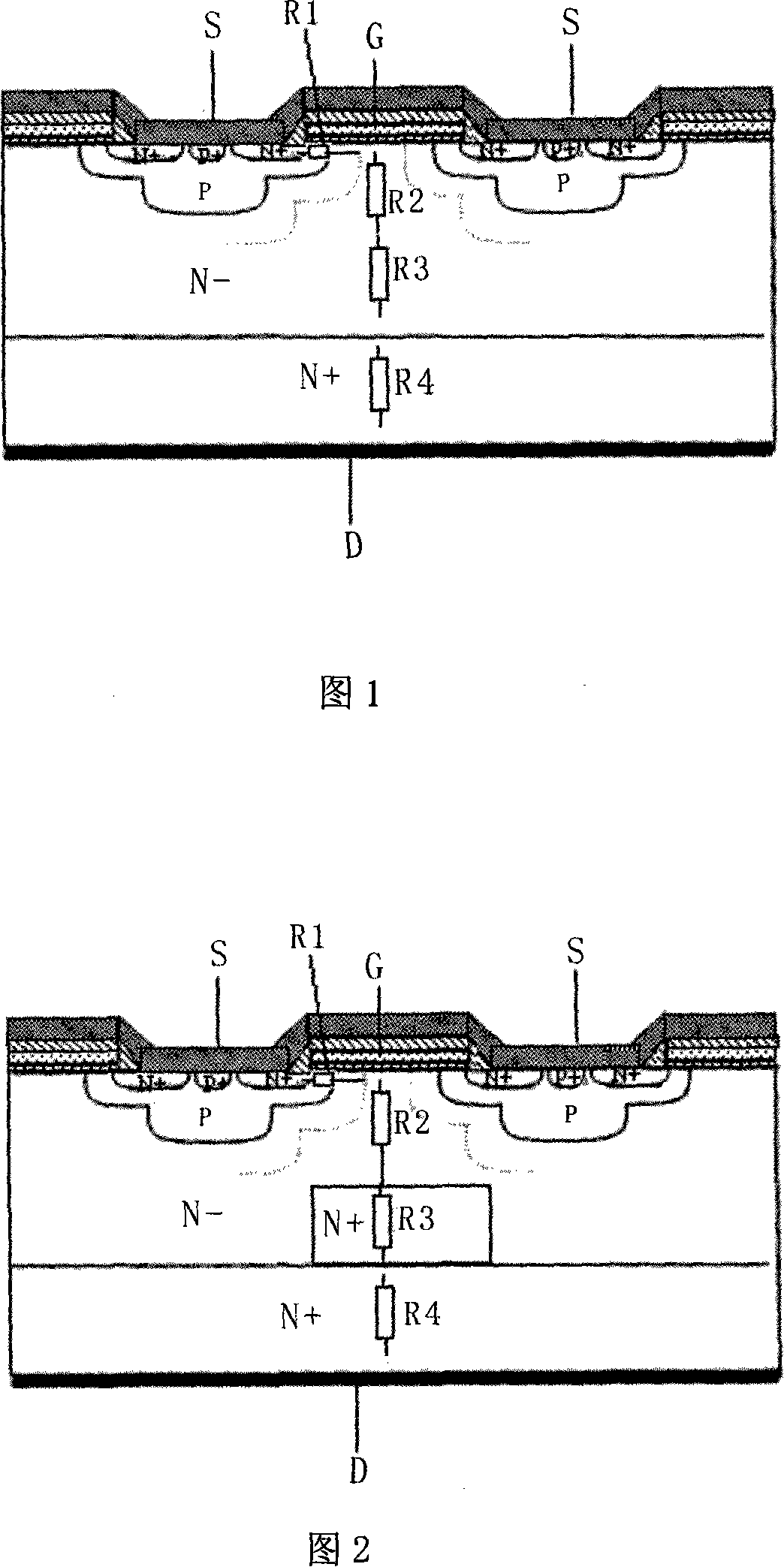
[0030] The specific embodiments of the present invention are not limited to the following description. The method of the present invention will be further described below in conjunction with the accompanying drawings.

[0031] The manufacturing method of the low on-resistance power VDMOS transistor of the present invention includes the following steps:

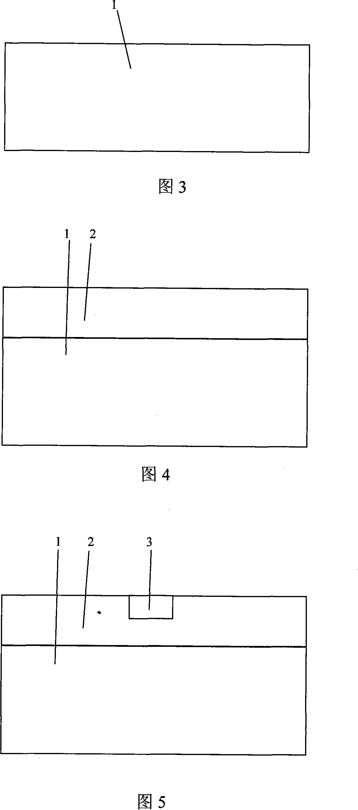
[0032]1. Prepare a 4-inch silicon single crystal with a resistivity of 0.0008-0.002Ω·cm and a thickness of 400-450μm with a P type crystal orientation as N + Silicon substrate sheet 1, as shown in Figure 3. After cleaning, in N + The epitaxial layer 2 with a thickness of 4-5 μm is grown on the silicon wafer, as shown in FIG. 4, and its resistivity is determined according to the breakdown voltage of the specific VDMOS tube. For a 100V breakdown VDMOS tube, the resistivity is usually 5-7Ω·cm.

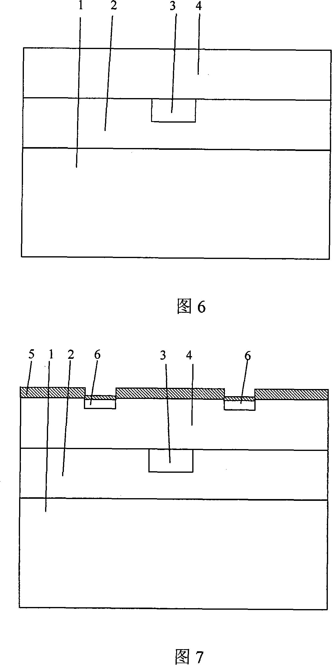
[0033] 2. After cleaning, grow SiO with a thickness of 950-1050nm 2 Layer; N required for photolithography + After cleaning, grow SiO with ...


PUM

PropertyMeasurementUnit
Thicknessaaaaaaaaaa

Abstract

This invention relates to a method for manufacturing low conductive resitance power VDMOS transistors, which reduces the conductive resistance just opposite to a channel of the drain end and between two VDMOS elements and adds a heavily doped N+ region in a region just under the grid of the VDMOS transistor in a first N- epitaxial layer on the N+ chip under the situation of meeting the pressure of the VDMOS transistor so as to reduce conductive resistance directly and radically.

Description

(1) Technical field [0001] The invention relates to a manufacturing method of a low on-resistance power MOS transistor, in particular to a manufacturing method of a low on-resistance power VDMOS transistor, and its direct application field is the field of VDMOS process manufacturing. (2) Background technology [0002] At present, the application fields of power devices are very wide, and they can be widely used in DC-DC converters, DC-AC converters, fast switching conversions, relays, motor drives, etc. In order to meet various needs, corresponding power devices have been developed: 1) Thyristor: The power control capacity is 10 7 Above W, the maximum operating frequency is 20kHz; 2) Power bipolar transistor: power control capacity up to 10 5 Above W, the maximum operating frequency is a few MHz; 3) Power MOS transistor: The power control capacity is only 10 2 Above W, the maximum operating frequency can reach dozens of MHz. Because the operating frequency of power MOS transistor...

Claims


Application Information

Patent Timeline
IPC IPC(8): H01L21/336
Inventor 张正元冯志成刘玉奎胡明雨郑纯
Owner NO 24 RES INST OF CETC
Why Eureka
Try Eureka