Method and device for transferring a chip to a contact substrate

A chip transfer and substrate technology, applied in the direction of electrical components, electrical solid devices, semiconductor/solid device manufacturing, etc., can solve problems such as long time

Active Publication Date: 2008-04-16
PAC TECH PACKAGING TECH
View PDF0 Cites 15 Cited by
  • Summary
  • Abstract
  • Description
  • Claims
  • Application Information

AI Technical Summary

Problems solved by technology

Chip processing requires complex equipment, and usually needs to be supplemented by other process steps to position each chip, so it takes a long time to complete the entire docking process

Method used


Image

  • Method and device for transferring a chip to a contact substrate
  • Method and device for transferring a chip to a contact substrate
  • Method and device for transferring a chip to a contact substrate

Examples


Embodiment Construction

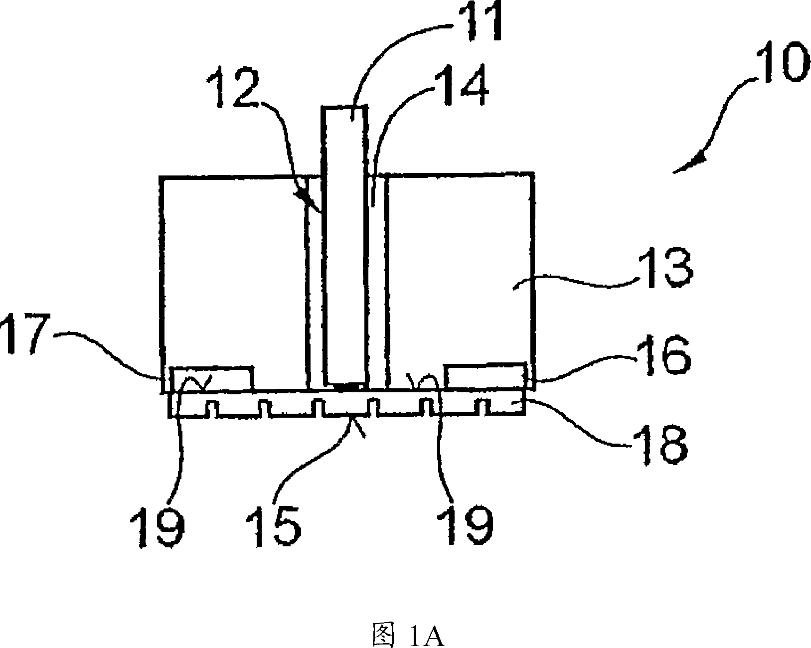
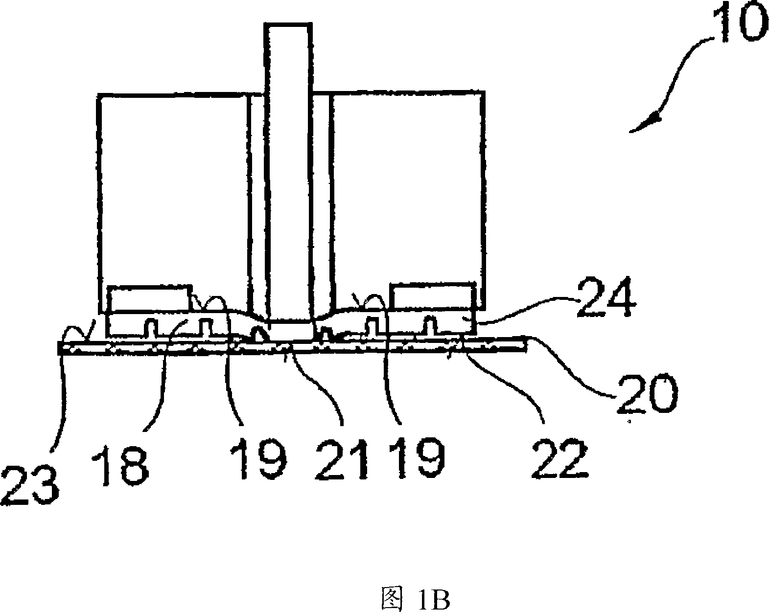
[0033] Referring to a simplified schematic diagram of an embodiment of the present invention, FIGS. 1A and 1B show a transfer tool 10 including a laser device in the form of an optical fiber 11 . The laser device can also serve as the pressing device 12 , and the optical fiber 11 can be guided in a channel 14 provided on the workpiece 13 . The lower front face of the workpiece 13 is arranged to contact a base positioning device 15 on which the foil 17 can be maintained through the vacuum opening 16 . A number of chips 18 are mounted on the foil 17 and the chips 18 are adhered to the foil 17 by means of an adhesive (not shown) between their back 19 and the foil 17 .

[0034] 1B shows a schematic diagram of the transfer process, the transfer tool 10 is located directly above a contact substrate 20, wherein the chip 18 opposite the free contact end 21 of the optical fiber 11 is pressed on the contact substrate 20 to conduct the chip 18 The contact gap 24 between the contact surf...


PUM


Abstract

A method and device for transferring a chip ( 18 ) situated on a transfer substrate ( 26 ) to a contact substrate ( 50 ), and for contacting the chip with the contact substrate, in which the chip, the back side ( 19 ) of which is attached adhesively to a support surface of the transfer substrate facing the contact substrate, is charged with laser energy from behind through the transfer substrate, and the chip contacts ( 59, 60 ) thereof that are arranged opposite a contact surface ( 58 ) of the contact substrate are brought into contact with substrate contacts ( 56, 57 ) arranged on the contact surface by means of a pressing device ( 45, 46 ) from behind through the transfer substrate, and a thermal bond is created between the chip contacts and the substrate contacts.

Description

technical field [0001] The invention relates to a method for transferring a chip on a transfer substrate to a contact substrate to form a butt joint between the chip and the contact substrate. Wherein, the back of the chip is attached to a supporting surface of the transfer substrate facing the contact base, and the laser energy is loaded on the chip from the back of the transfer substrate. Through a pressing device, the chip contact arranged opposite to the contact surface contacting the substrate is docked with the substrate contact arranged on the contact surface, and a thermal bonding layer is formed between the chip contact and the substrate contact. The invention also relates to a device for carrying out the aforementioned method. Background technique [0002] The chip on the substrate usually needs to be processed to position the chip and the substrate relative to each other before the actual docking operation, so that the corresponding arrangement of the chip contac...

Claims


Application Information

Patent Timeline
Patent Type & Authority Applications(China)
IPC IPC(8): H01L21/60
CPCH01L21/6836H01L2224/75314H01L2224/293H01L2221/68354H01L21/67144H01L21/6835H01L21/67132H01L2924/014H01L2224/81224H01L2224/75263H01L2224/16H01L2224/83851H01L2224/81005H01L24/86H01L24/31H01L24/83H01L2924/01033H01L2924/01082H01L2224/81801H01L24/75H01L2924/01079H01L2221/68327H01L2224/7965H01L2224/83192H01L2224/75H01L2924/01006H01L2224/2929H01L2924/19043H01L2224/7565H01L24/81H01L2224/75317H01L2224/81193H01L2224/83005H01L2924/00014
Inventor E·扎克尔G·阿特达斯特
Owner PAC TECH PACKAGING TECH
Why Eureka
Try Eureka