
Eureka
For R&D, Eureka makes reading and utilizing patents & technical documents easy.
Eureka AIR
Designed for self-driven R&D workflows. Generate viable solutions, solve complex R&D challenges, empower your innovation with AI.

Eureka Materials
Designed for material experts only. Revolutionize your material R&D, from search, analyze, to developing new materials.

TechResearch
Generate reliable direction feasibility study reports for your R&D in just a few steps.

TechSeek
Discover and master advanced knowledge NOW. Basics, ideas, possibilities, all at once.

TechMind
As an expert in R&D Theories, TechMind can generates customized viable solutions instantly.

TechRisk
Analyze your overall solution with one click, know your potential R&D risks in advance.

TechMonitor
Get weekly tech updates, stay abreast of the latest tech innovations and key insights.
Pixel structure capable of avoiding black-white point flickering after laser repairing
A pixel structure and semiconductor technology, applied in optics, nonlinear optics, instruments, etc., can solve the problems of flicker and reduce the image display quality of thin film transistor liquid crystal displays, and achieve the effect of improving repair quality and efficiency
- Summary
- Abstract
- Description
- Claims
- Application Information
AI Technical Summary
Problems solved by technology
Method used
Image

Examples
Embodiment Construction
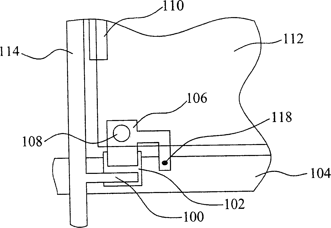
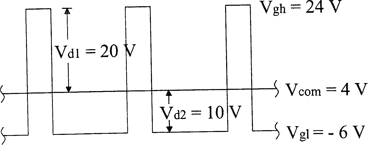
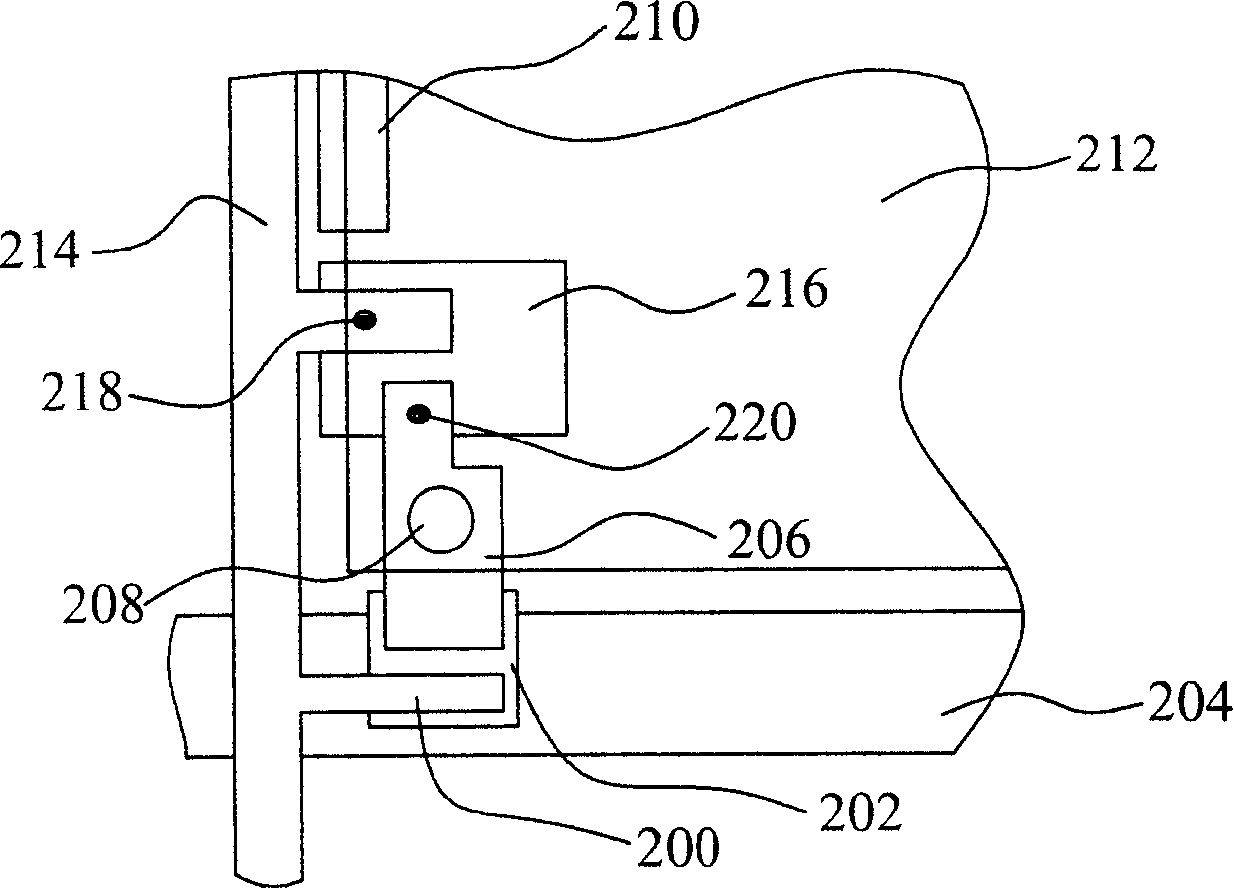
[0033] Figure 3AIt is a partial top view of the laser repaired pixel structure in the first embodiment of the present invention. The pixel of the thin film transistor array substrate has a multi-layer structure, and has two metal layers of a gate electrode layer and a source / drain electrode layer. The gate electrode The layer includes a gate line 304, a storage capacitor line 310 and a first floating metal 316. The gate line 304 is arranged along a row, the storage capacitor line 310 transmits a common voltage Vcom, and the source / drain electrode layer Including a source line 314, a source electrode 300 and a drain electrode 306, the source line 314 transmits the source signal to the source electrode 300, the source electrode 300 and the drain electrode 306 are respectively connected to a first semiconductor electrode 302 Partially overlapping, the gate line 304 has a gate electrode (not shown) located below the first semiconductor electrode 302 , and the gate signal is trans...
PUM
 Abstract
Description
Claims
Application Information
 - R&D Engineer
- R&D Manager
- IP Professional
- Industry Leading Data Capabilities
- Powerful AI technology
- Patent DNA Extraction
Browse by: Latest US Patents, China's latest patents, Technical Efficacy Thesaurus, Application Domain, Technology Topic, Popular Technical Reports.
© 2024 PatSnap. All rights reserved.Legal|Privacy policy|Modern Slavery Act Transparency Statement|Sitemap|About US| Contact US: help@patsnap.com