Color filter and method for manufacturing the same

A technology for a color filter and a manufacturing method, applied in the field of color filters, can solve the problems of affecting the thickness of the color filter, unable to use an array substrate, etc., and achieve the effects of good film thickness uniformity and cost reduction

Inactive Publication Date: 2008-04-23
CHUNGHWA PICTURE TUBES LTD
View PDF0 Cites 9 Cited by
  • Summary
  • Abstract
  • Description
  • Claims
  • Application Information

AI Technical Summary

Problems solved by technology

The use of inkjet technology on the array substrate still needs to consider the design of the retaining wall. Because the thickness of the color layer is about 1.4 microns or more, it cannot be manufactured using the film thickness of the components on the ar

Method used


Image

  • Color filter and method for manufacturing the same
  • Color filter and method for manufacturing the same
  • Color filter and method for manufacturing the same

Examples


Embodiment Construction

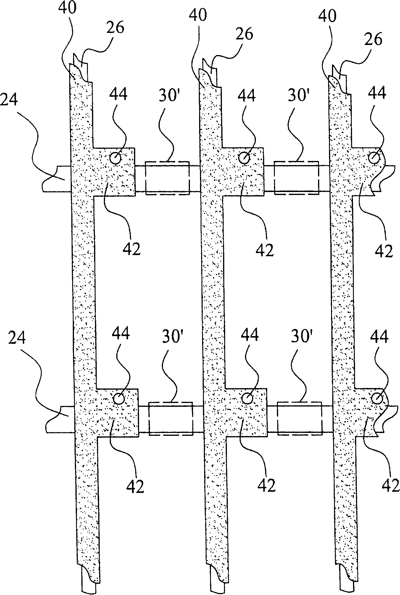
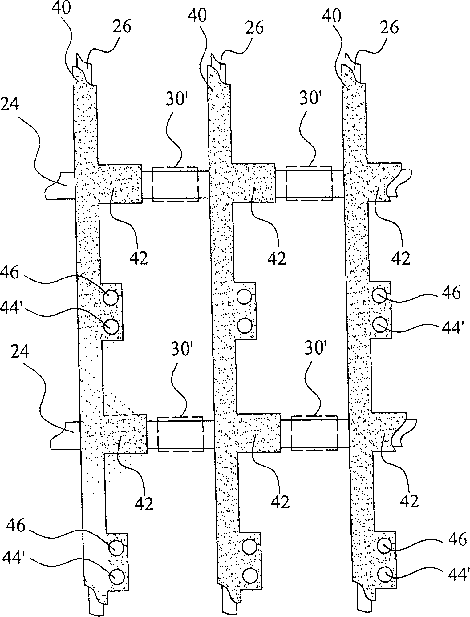
[0029] Figure 1A and Figure 1B Shown is a partial plan view of different embodiments of the manufacturing method and structure of the color filter of the present invention. refer to Figure 1A , in this embodiment, a plurality of signal lines 26 and a plurality of scanning lines 24 are intersected and arranged on a substrate (not shown in the figure) to define a plurality of pixel regions, and thin film transistors are arranged on the scanning lines of each pixel region, As shown at 42 where the thin film transistor is disposed. The patterned light-shielding layer 40 is used to cover the thin film transistor and metal lines connected to the thin film transistor, such as the signal line 26 . There is an insulating layer (not shown in the figure) between the patterned light-shielding layer 40 and the TFT array, and the patterned light-shielding layer 40 exposes a contact window 44 of the TFT.

[0030] Continuing from the above-mentioned embodiment, such as Figure 1A As show...


PUM


Abstract

The method comprises: providing a baseboard; setting up a thin film transistor array on the baseboard; forming an insulating layer on the thin film transistor array; removing the insulation layer in order to reduce the thickness of the insulation layer located in the scan line area between the transistors; setting up a patterned light shading layer on the insulation layer; forming a color filtering layer on the insulation layer; the patterned light shading layer is around the color filter layer; forming a transparent conducting layer on the color filter layer.

Description

technical field [0001] The invention relates to a color filter, in particular to a color filter and a manufacturing method thereof. Background technique [0002] Due to the advantages of high image quality, small size, light weight, low voltage drive, low power consumption and wide application range, liquid crystal displays have been widely used in electronic product display devices, such as portable TVs, mobile phones, video recording Consumer electronics or computer products such as laptops, laptops, and desktop monitors have become the mainstream of displays. The production of general thin film transistor liquid crystal display can be roughly divided into thin film transistor array (TFT array) process, color filter (color filter) process, liquid crystal display unit assembly (liquid crystal cell assembly) process, and liquid crystal display module (liquid crystal module) Process. [0003] The thin film transistor array process is used to manufacture the thin film transi...

Claims


Application Information

Patent Timeline
IPC IPC(8): H01L21/84H01L27/12G02F1/136
Inventor 李得俊吴德俊方斯郁
Owner CHUNGHWA PICTURE TUBES LTD
Why Eureka
Try Eureka