

Semiconductor packaging member for semiconductor device stacking and its manufacture method
A semiconductor and packaging technology, applied in the field of ball grid array semiconductor packaging, can solve the problems of increasing the cost of semiconductor packaging, increasing the complexity of the packaging process, reliability and quality issues, and achieving the goal of improving reliability and quality Effect
Active Publication Date: 2010-11-10
SILICONWARE PRECISION IND CO LTD
View PDF3 Cites 0 Cited by
- Summary
- Abstract
- Description
- Claims
- Application Information
AI Technical Summary
Problems solved by technology
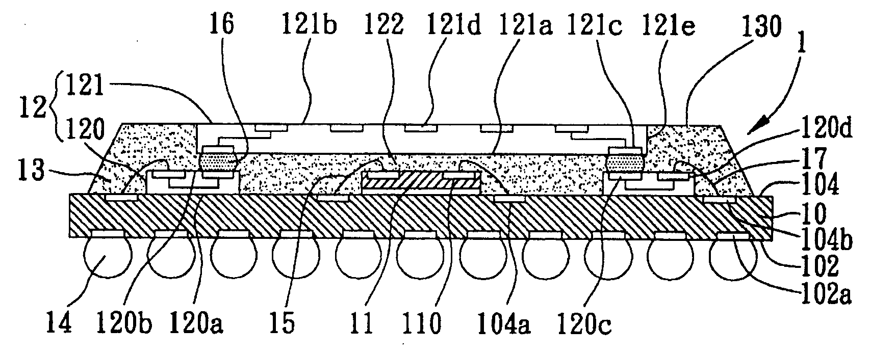
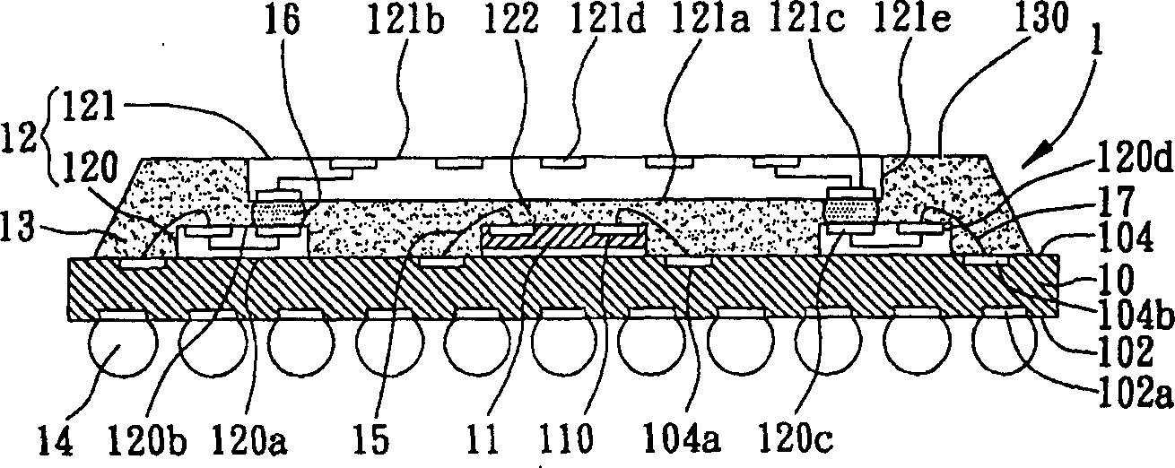
Although the circuit board 92 of the semiconductor package 9 does not need to be electrically connected to the substrate 91 through solder balls, the circuit board 92 must be mounted on the chip 93 using a metal carrier 90, which not only increases the complexity of the packaging process, but also Cause the increase of cost; Simultaneously, this circuit board 92 is combined with metal carrier 90 surface and surface (Surface-to-Surface), metal carrier 90 and spacer 94 surface-to-surface combination, and spacer 94 and chip 93 surface Combined with the surface, the semiconductor package 9 has multiple interfaces (Interface) in contact with the surface, so that the semiconductor package 9 is easy to be at the interface during the temperature cycle (Temperature Cycle) of the process and the working state after manufacture. Delamination occurs, resulting in reliability and quality problems of the product; in addition, the second welding wire 98 that is higher than the exposed top surface 920 of the circuit board 92 for the cladding wire loop height (HeightofWireLoop), and makes the circuit The welding pad 921 on the board 92 can expose the encapsulation compound 95. As shown in FIG. The second welding wire 98 is higher than the part of the exposed top surface 920 of the circuit board 92. The use of the upper mold M1 with a special specification will increase the cost of making the semiconductor package 9.
Method used
View moreImage
Smart ImageViewing Examples

Examples
no. 1 example
no. 2 example
no. 3 example
Login to View More PUM
 Abstract
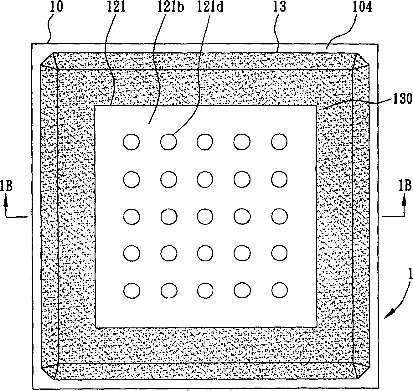
The method comprises: setting up and electrically-connecting at least on semiconductor chip; through an electrical connection structure composed of an upper layer circuit board and lower layer circuit board, the semiconductor chip is connected to the baseboard; said semiconductor chip is held by a holding space in the electrical connection structure; forming a sealing gel used for covering the semiconductor chip and the electrically connection structure; after completing the forming of sealing gel, multi weld pads are exposed from the sealing gel in order to make at least one semiconductor component electrically connected to the upper layer circuit board so as to form a stack structure.
Description
Semiconductor package on which semiconductor devices can be stacked and its manufacturing method technical field The invention relates to a semiconductor package, in particular to a ball grid array (BGA, BallGridAway) type semiconductor package. Background technique In addition to the miniaturization of electronic products, performance and processing speed are still required to be improved. The best way to improve performance and processing speed is nothing more than increasing the number or size of chips in the semiconductor package, but the area available on the substrate for chip connection is often not enough for multiple chips to be arranged horizontally or larger in size. chip placement. Therefore, the current development focuses on the stackable multi-chip module (stakable multi-chip module) in which multiple chips are stacked up and down. The structure of this stacked multi-chip module, as shown in U.S. Patent No. 5,222,014, an upper semiconductor package is sta...
Claims
Login to View More Application Information
Patent Timeline
 Patent Type & AuthorityPatents(China)
IPC IPC(8): H01L23/488H01L23/31H01L21/60H01L21/56H01L21/50H05K1/14H05K3/36
CPCH01L2924/19107H01L2924/15321H01L2224/32225H01L21/565H01L2224/16225H01L2224/48227H01L2924/15311H01L2224/73265H01L2224/45144H01L24/73H01L2924/00012H01L2924/00
Inventor普翰屏黄建屏黄致明王愉博萧承旭
OwnerSILICONWARE PRECISION IND CO LTD