Pixel structure and liquid crystal display panel using same

A liquid crystal display panel and pixel structure technology, applied in static indicators, nonlinear optics, optics, etc., can solve the problems of reducing panel brightness, sacrificing aperture ratio, etc., and achieve the effect of high aperture ratio

Inactive Publication Date: 2008-04-30
CHUNGHWA PICTURE TUBES LTD
View PDF4 Cites 7 Cited by
  • Summary
  • Abstract
  • Description
  • Claims
  • Application Information

AI Technical Summary

Problems solved by technology

In the liquid crystal display disclosed in the above three patents, although the transition initiation point can be generated by the transverse electric field, however, the method of digging a hole (slit) in the pixel electrode of the liquid crystal display will sacrifice the aperture ratio and reduce the brightness of the panel and other shortcomings

Method used


Image

  • Pixel structure and liquid crystal display panel using same
  • Pixel structure and liquid crystal display panel using same
  • Pixel structure and liquid crystal display panel using same

Examples


Embodiment Construction

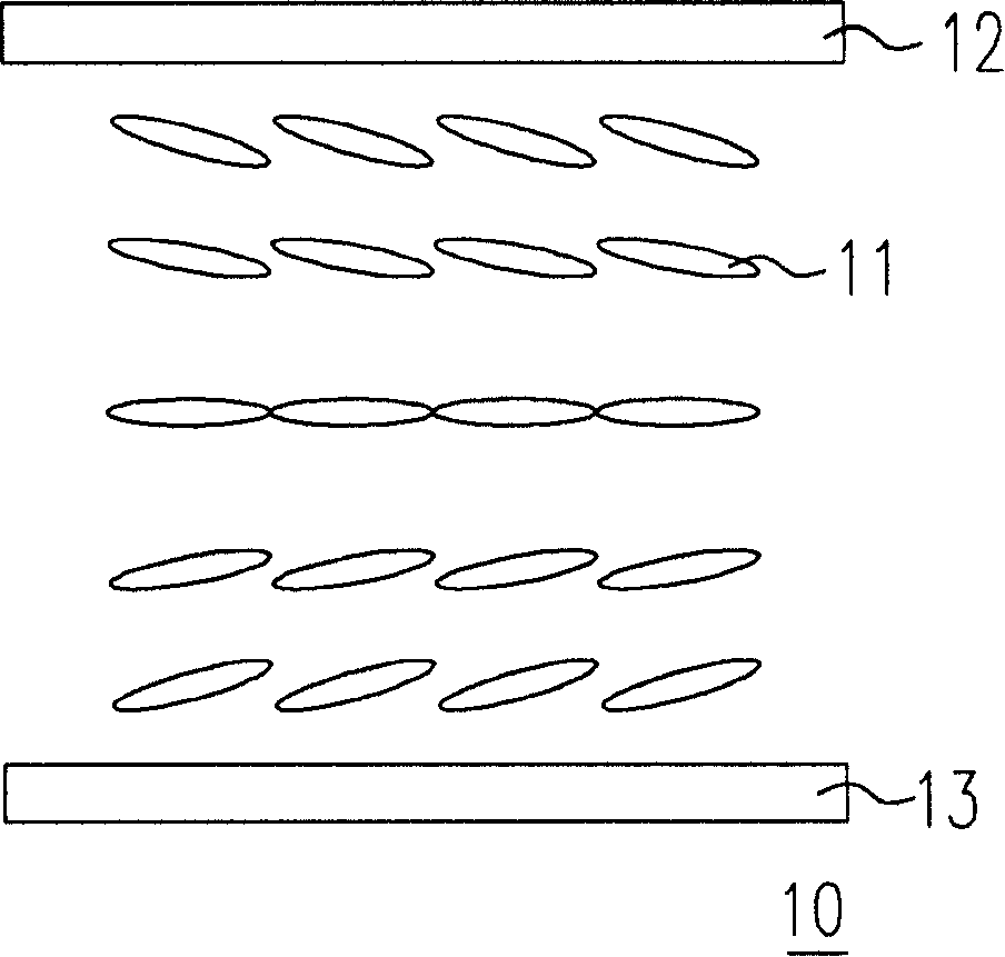
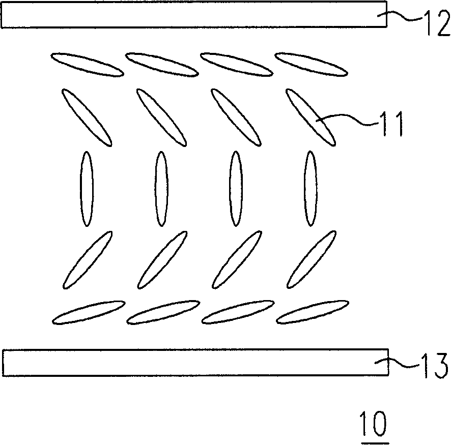
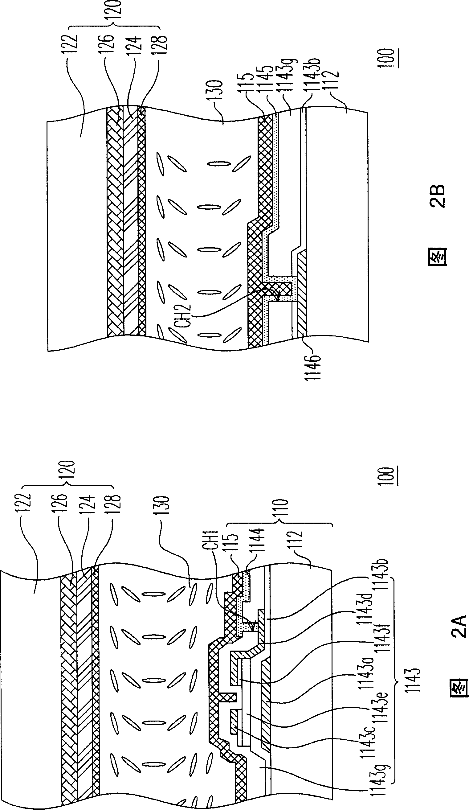
[0028] 2A and 2B are schematic diagrams showing a partial cross-sectional structure of a liquid crystal display panel according to an embodiment of the present invention; Figure 2C A top view of the active element array substrate in the liquid crystal display panel shown in FIGS. 2A and 2B, wherein FIG. 2A is Figure 2C The cross-sectional schematic diagram drawn along the I-I' section line in Fig. 2B is Figure 2C The cross-sectional schematic diagram drawn along the ∏-∏′ section line in . Please refer to FIGS. 2A , 2B and 2C at the same time. The liquid crystal display panel 100 is an optically compensated birefringence type liquid crystal display panel, which includes an active device array substrate 110 , a color filter substrate 120 and a liquid crystal layer 130 . The color filter substrate 120 is disposed above the active device array substrate 110 , and the liquid crystal layer 130 is sandwiched between the color filter substrate 120 and the active device array subst...


PUM


Abstract

The invention relates to a pixel structure which comprises a base plate, a scanning wiring, a data wiring, a common wiring, an active element, a pixel electrode, a protective layer and a rotating state auxiliary electrode. The scanning wiring and the data wiring are crossly arranged on the base plate, and a pixel area is defined on the base plate. The common wiring is arranged on the base plate and is virtually parallel with the scanning wiring. The active element is arranged in the pixel area, and is electrically connected with the scanning wiring and the data wiring. The pixel electrode is arranged in the pixel area and is electrically connected with the active element. The protective layer is arranged between the pixel electrode and the data wiring. The rotating state auxiliary electrode is arranged around the pixel electrode, and the pixel electrode and the rotating state auxiliary electrode share the same film layer. In addition, the rotating state auxiliary electrode permeates a touching window of the protective layer to electrically connect with the common wiring.

Description

technical field [0001] The present invention relates to a pixel structure and a display panel, and in particular to a pixel structure and a liquid crystal display panel suitable for an optically compensated birefringence liquid crystal display (OCB LCD). Background technique [0002] As the demand for displays is increasing day by day, the industry is fully committed to the development of related displays. Among them, the cathode ray tube (CRT) has monopolized the display market for many years because of its excellent display quality and technological maturity. However, due to the rise of the concept of green environmental protection recently, based on the characteristics of large energy consumption and large radiation generated by cathode ray tubes, and the limited space for flattening their products, cathode ray tubes cannot meet the market demand for light, thin, short , small, beautiful and low power consumption market trends. Therefore, a thin film transistor liquid c...

Claims


Application Information

Patent Timeline
IPC IPC(8): G02F1/133G02F1/1343G02F1/1362
Inventor 王智杰简耀黉林兟兟陈丽珊刘轩育
Owner CHUNGHWA PICTURE TUBES LTD
Why Eureka
Try Eureka