MOS transistor radio frequency circuit simulated macro model and its parameter extraction method

A technology of MOS transistors and radio frequency circuits, which is used in electrical digital data processing, special data processing applications, instruments, etc., and can solve problems such as unsatisfactory performance effects.

Active Publication Date: 2008-04-30
SHANGHAI INTEGRATED CIRCUIT RES & DEV CENT
View PDF0 Cites 18 Cited by
  • Summary
  • Abstract
  • Description
  • Claims
  • Application Information

AI Technical Summary

Problems solved by technology

At present, the "Π" type three-resistor network configuration method is widely used, and the specific structure is shown in Figure 1. This model mainly includes MOSFET 1' and three resistors R 1 , R 2 , R 3 and tw

Method used


Image

  • MOS transistor radio frequency circuit simulated macro model and its parameter extraction method
  • MOS transistor radio frequency circuit simulated macro model and its parameter extraction method
  • MOS transistor radio frequency circuit simulated macro model and its parameter extraction method

Examples


Embodiment Construction

[0031] The MOS transistor radio frequency circuit simulation macro model and its parameter extraction method of the present invention will be further described in detail below.

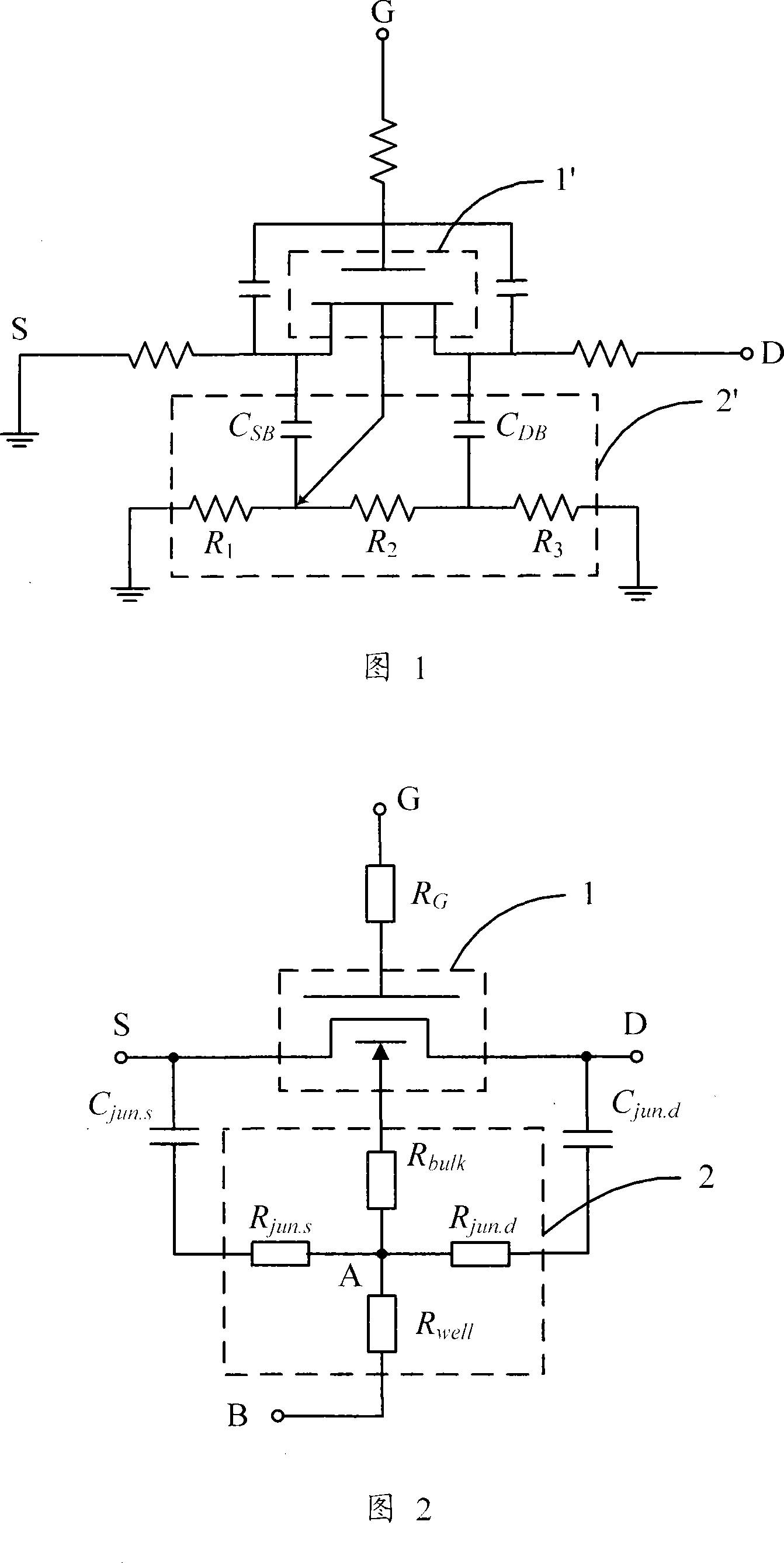
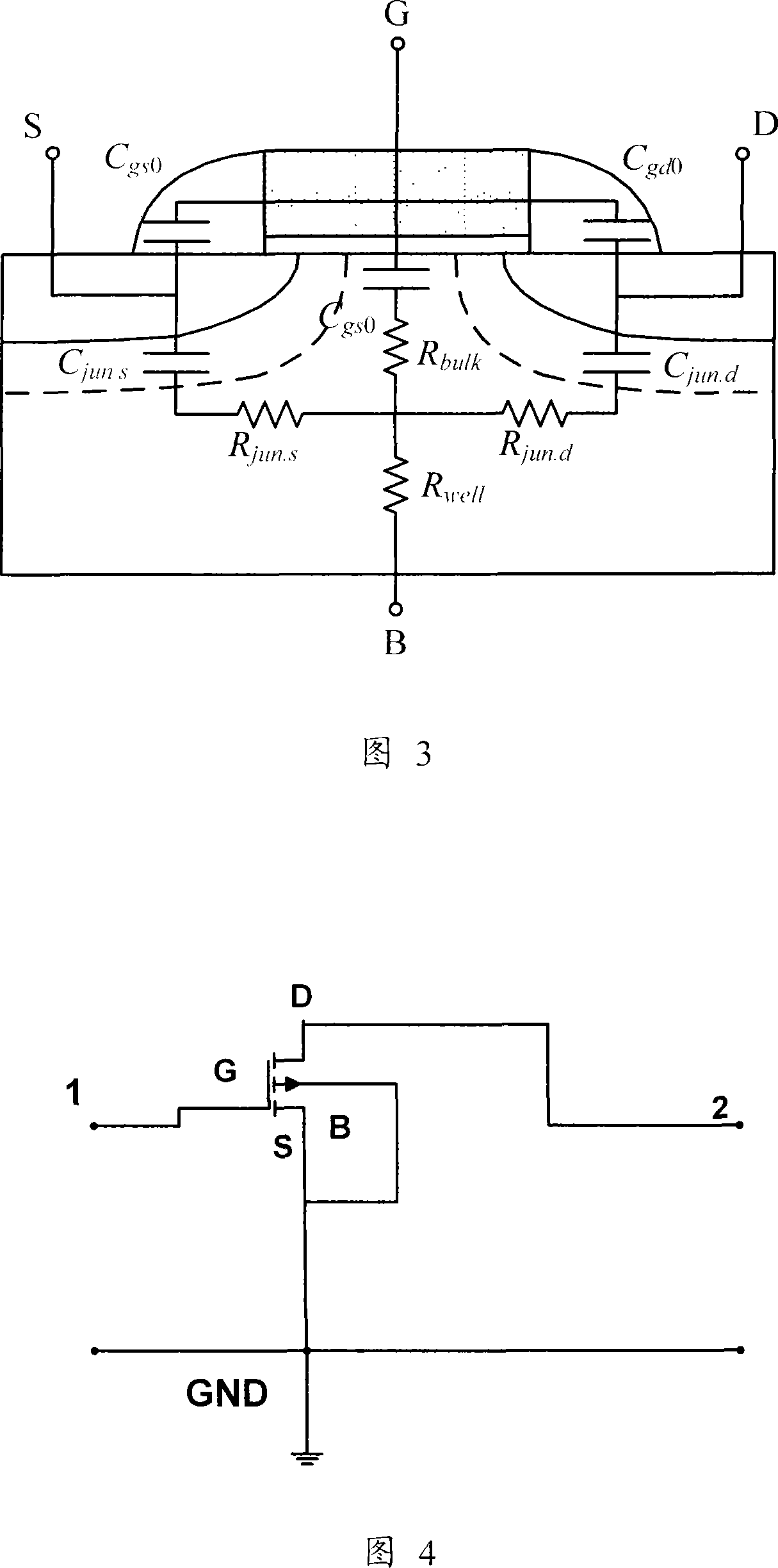
[0032] As shown in FIG. 2 , the present invention utilizes a MOS transistor radio frequency circuit simulation macro model to simulate a MOS transistor radio frequency circuit, and the simulation circuit has a gate node G, a source node S, a drain node D and a substrate node B. The MOS transistor radio frequency circuit simulation macro model includes a MOS transistor simulation model 1, a MOS transistor gate connected in series with the simulation circuit gate node G, used to characterize the gate resistance R between the transistor gate and the contact hole electrode G , the source junction capacitance C used to characterize the junction capacitance and parasitic resistance between the source and substrate jun.s with the first substrate resistance R jun.s , the drain junction capacitance C used to ...


PUM


Abstract

The invention provides a MOS transistor radio-frequency circuit simulation macro model and a parameter extraction method thereof. The simulation macro model comprises a MOS transistor simulation model, a gate resistor RG connected between a transistor gate node and a circuit grate node in series, a capacitor Cjun.s and a resistor Rjun.s and a capacitor Cjun.d and a resistor Rjun.d respectively indicating the a source electrode and a substrate, as well as the junction capacitance and parasitic resistance therebetween, and two resistor Rbulk and Rwell respectively indicating bulk resistance and trap resistance of the transistor. The four resistors Rjun.s, Rjun.d, Rbulk and Rwell are connected at one point, and indicate the parasitic resistance introduced by the substrate with a T-shaped structure. The invention also provides a method for extracting parameters of each element of a substrate network structure in the macro model using the equivalent circuit Y-parameter analytic method. The invention simulation macro model is suitable for frequency up to 20GHz, improves model accuracy of the MOS transistor in 20GHz high frequency domain, and expands the frequency application range of CMOS circuit EDA design.

Description

technical field [0001] The invention belongs to the field of integrated circuits, in particular to a MOS transistor radio frequency circuit simulation macro model and a method for extracting substrate network structure parameters. Background technique [0002] With the increasing application of CMOS technology in the radio frequency (RF) field, the accuracy of high frequency models of MOS devices is becoming more and more important for RF product design. Since the parasitic effects of MOS devices are more complex at high frequencies and have a greater correlation with the layout, the current practice is to build high-frequency models for MOS devices in the form of macro models. [0003] The BSIM3 SPICE model is an industry standard for CMOS models, but it has significant deficiencies in both simulation and RF performance. Its RF model does not include non-quasistatic effects, and the model structure does not include gate resistors and substrate resistor networks. Therefore,...

Claims


Application Information

Patent Timeline
IPC IPC(8): G06F17/50
Inventor 胡少坚任铮
Owner SHANGHAI INTEGRATED CIRCUIT RES & DEV CENT
Why Eureka
Try Eureka