4-end transistor substrate resistance network model
A technology of substrate resistance and network model, which is applied in the fields of electrical digital data processing, special data processing applications, instruments, etc., can solve problems such as unsatisfactory performance and effect
- Summary
- Abstract
- Description
- Claims
- Application Information
AI Technical Summary
Problems solved by technology
Method used
Image


Examples
Embodiment Construction
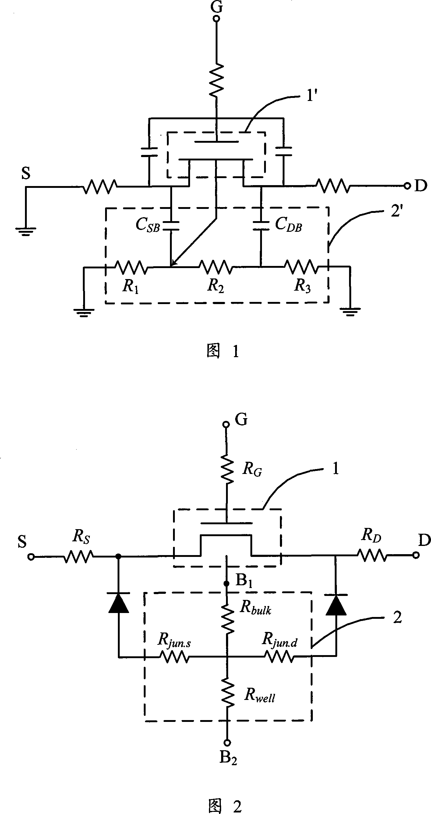
[0032] The variable size model of the four-terminal transistor substrate resistor network of the present invention will be further described in detail below.
[0033] The substrate resistance network model of the present invention can be applied to the four-terminal transistor with substrate and well structure similar to the MOS FET transistor, for example: high voltage MOS FET (VD-MOS, LD-MOS) or JFET junction field effect transistor In the equivalent circuit macro model, the radio frequency MOS transistor is only used as a preferred embodiment of the present invention for illustration below.
[0034] As shown in Figure 2, the RF MOS transistor equivalent circuit has an external substrate node B 2 and an internal MOS transistor 1 having a gate G, a source S, a drain D and a substrate electrode B 1 . The substrate resistor network 2 consists of four resistors, including a source S and a substrate electrode B for characterizing 1The parasitic resistance between R jun.s , us...
PUM
 Abstract
Description
Claims
Application Information
 - R&D
- Intellectual Property
- Life Sciences
- Materials
- Tech Scout
- Unparalleled Data Quality
- Higher Quality Content
- 60% Fewer Hallucinations
Browse by: Latest US Patents, China's latest patents, Technical Efficacy Thesaurus, Application Domain, Technology Topic, Popular Technical Reports.
© 2025 PatSnap. All rights reserved.Legal|Privacy policy|Modern Slavery Act Transparency Statement|Sitemap|About US| Contact US: help@patsnap.com