Method for thinning display panel device

A display panel and thinning technology, which is applied in the field of thinned display panel devices, can solve the problems of substrate thinning technology limitations, fragmentation, and easy bending of the substrate

Inactive Publication Date: 2008-06-18
AU OPTRONICS CORP
View PDF0 Cites 21 Cited by
  • Summary
  • Abstract
  • Description
  • Claims
  • Application Information

AI Technical Summary

Problems solved by technology

[0004] However, existing substrate thinning techniques still have their limitations
Once the substrate is thinned below a certain thickness, the substrate is prone to warp, and the thinning manufacturing process cannot be continued at this time, otherwise it will affect the overall flatness of the liquid crystal display panel and may cause fragments; for example, the existing Advanced substrate thinning technology, if using hydrofluoric acid (HF) solution, the glass substrate can only be etched from 0.5 millimeters (mm) to 0.3 millimeters (mm), and it can no longer be thinned, otherwise it will affect the flatness of the glass substrate cause adverse effects, the thinning effect of the prior art does have its limits

Method used


Image

  • Method for thinning display panel device
  • Method for thinning display panel device
  • Method for thinning display panel device

Examples


Embodiment Construction

[0027] In order to make the above-mentioned purpose, technical features, and advantages of the present invention more comprehensible, preferred embodiments are described below in detail with accompanying drawings.

[0028] The following embodiments and drawings are used to illustrate the content of the present invention, but not to limit the present invention.

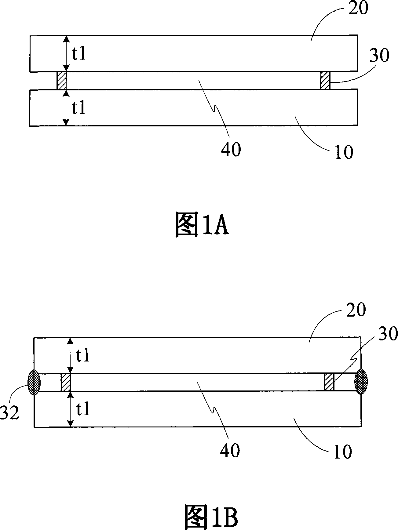
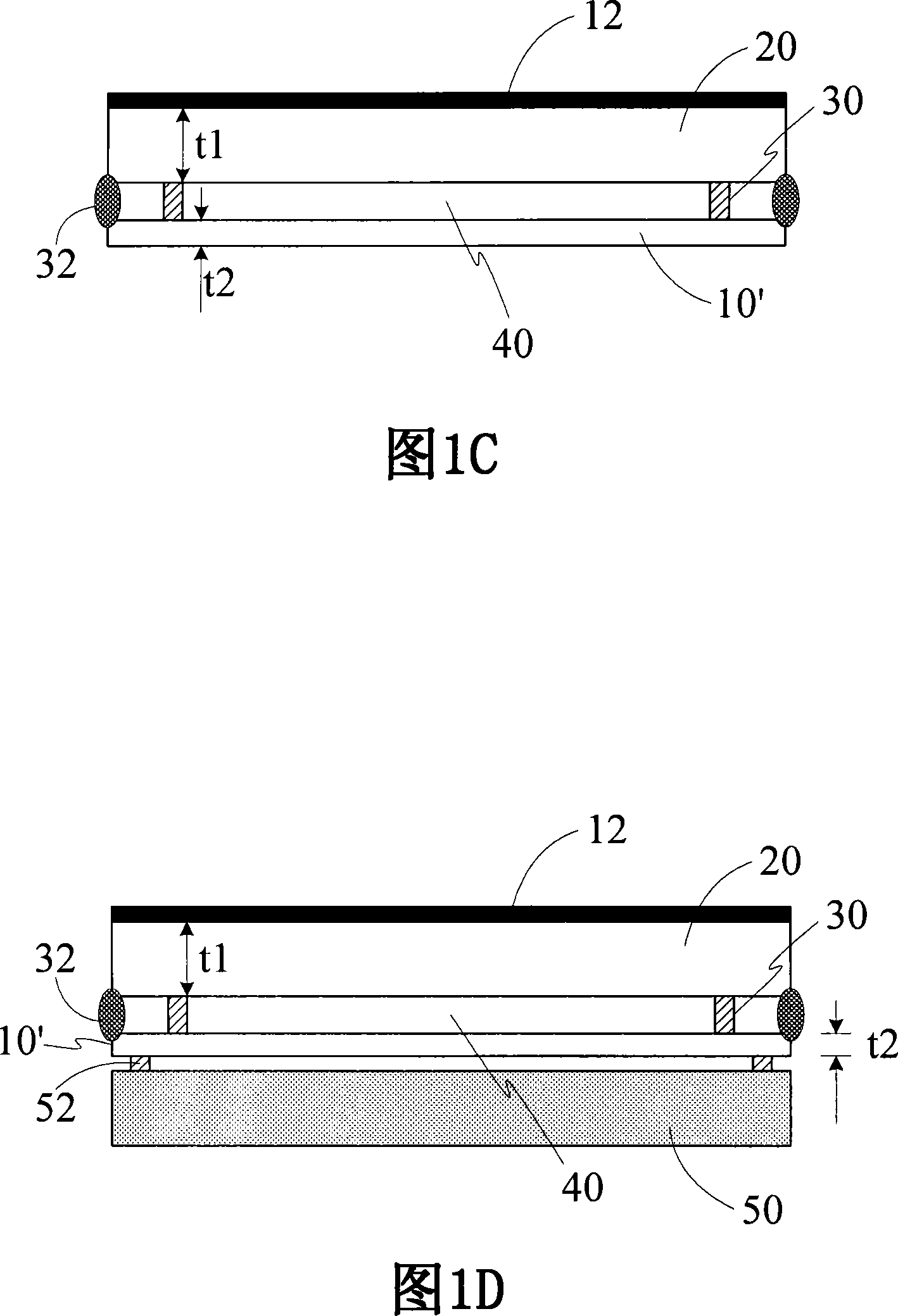
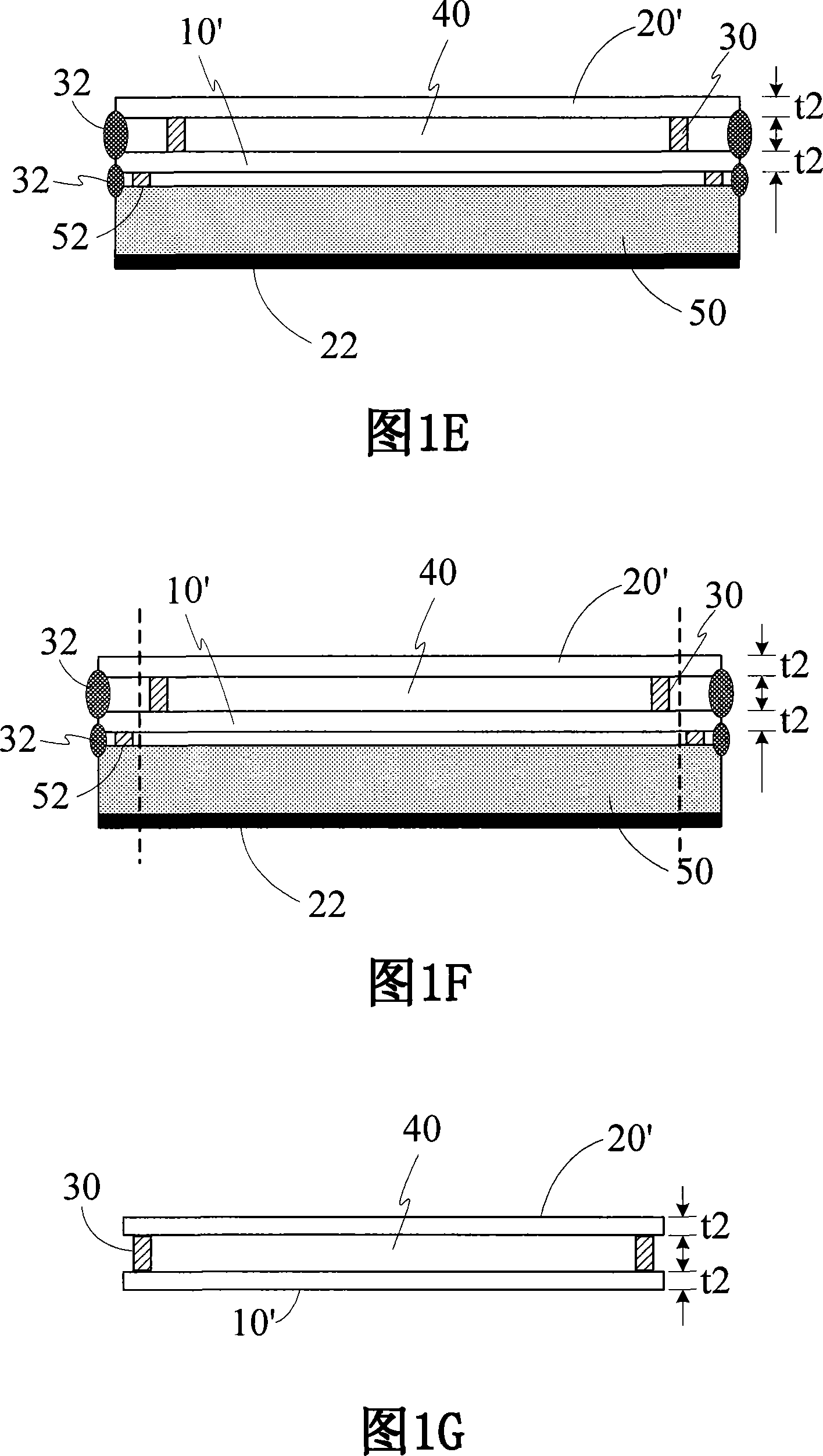
[0029] Please refer to FIG. 1A to FIG. 1G first. FIG. 1A to FIG. 1G are schematic views of an embodiment of a method for thinning a display panel device of the present invention. In this embodiment, the display panel device includes a first substrate 10 and a second substrate 20 , and the first substrate 10 and the second substrate 20 are firstly assembled with each other. Wherein, an array of thin film transistors may be formed on the first substrate 10 , for example, at least one switch element and at least one pixel electrode, and the second substrate 20 , for example, a color filter layer may be formed thereon. Th...


PUM


Abstract

The invention relates to a method for thinning a display panel device; the display panel device comprises a first substrate and a second substrate. The method for thinning the display panel device comprises the following steps: firstly, the first substrate is thinned and the thinned first substrate is supported by a bearing device, secondly, the second substrate is thinned. The manufacturing method of the invention can provides better thinning effect and can meet the requirement of mass production.

Description

technical field [0001] The present invention relates to a method for manufacturing a display panel device, in particular to a method for thinning a display panel device. Background technique [0002] Due to the continuous progress of optoelectronic technology in recent years, coupled with the entry of image display technology into the digital age, the liquid crystal display market has been vigorously developed. Liquid crystal displays are widely used in personal digital assistants (PDAs), mobile phones, camcorders, notebook computers, desktop monitors, On top of consumer communication or electronic products such as car displays and projection TVs, and gradually replacing traditional cathode ray tubes, it has become the mainstream in the display market. [0003] Among them, a key zero component of the liquid crystal display is the liquid crystal display panel. Nowadays, in addition to the pursuit of large size, the manufacturing technology of liquid crystal display panels i...

Claims


Application Information

Patent Timeline
Patent Type & Authority Applications(China)
IPC IPC(8): G02F1/1333B24B9/10C03C15/00
Inventor 储中文刘昱辰林朝成吴哲耀
Owner AU OPTRONICS CORP
Why Eureka
Try Eureka