Semiconductor device and method of manufacturing such a device

A semiconductor and silicon semiconductor technology, applied in semiconductor/solid-state device manufacturing, semiconductor devices, electrical components, etc., and can solve problems such as crosstalk

Inactive Publication Date: 2011-09-07
NXP BV
View PDF1 Cites 0 Cited by
  • Summary
  • Abstract
  • Description
  • Claims
  • Application Information

AI Technical Summary

Problems solved by technology

[0003] A disadvantage of the known transistors is that in the case of MOS transistors the transistors exhibit a number of unfavorable phenomena, among them crosstalk

Method used


Image

  • Semiconductor device and method of manufacturing such a device
  • Semiconductor device and method of manufacturing such a device
  • Semiconductor device and method of manufacturing such a device

Examples


Embodiment Construction

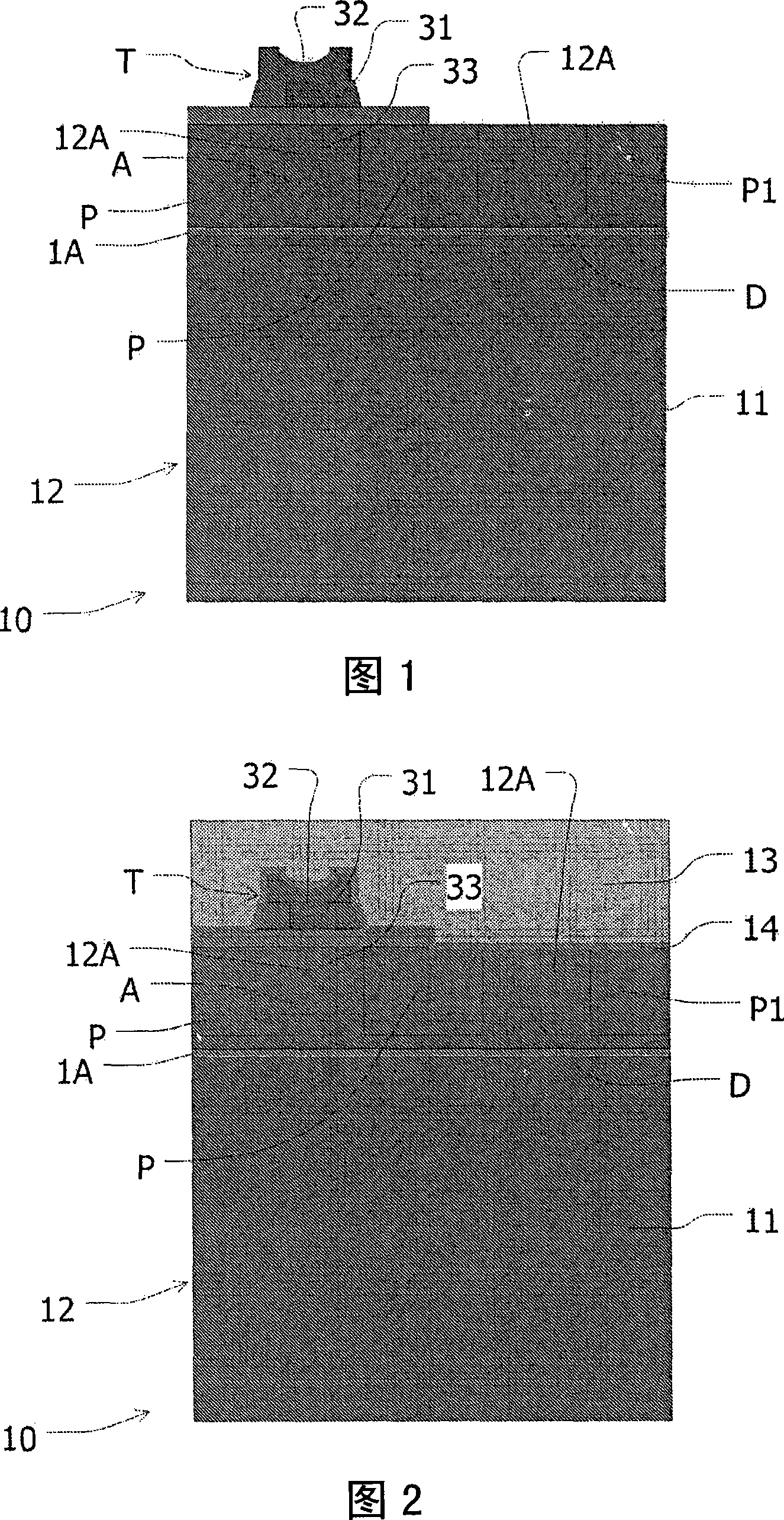
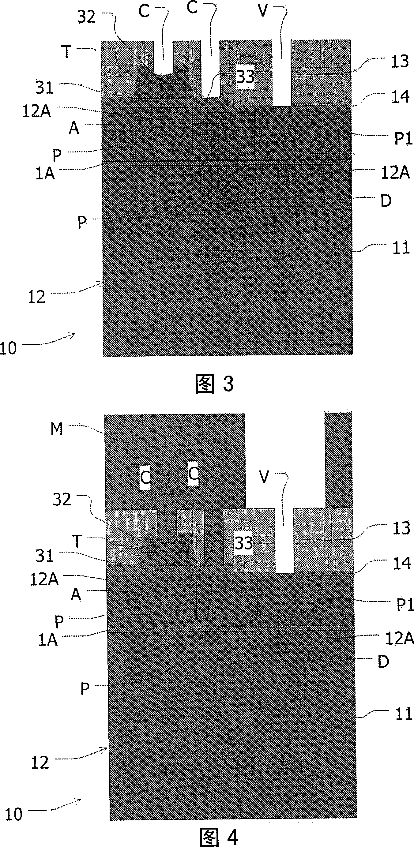
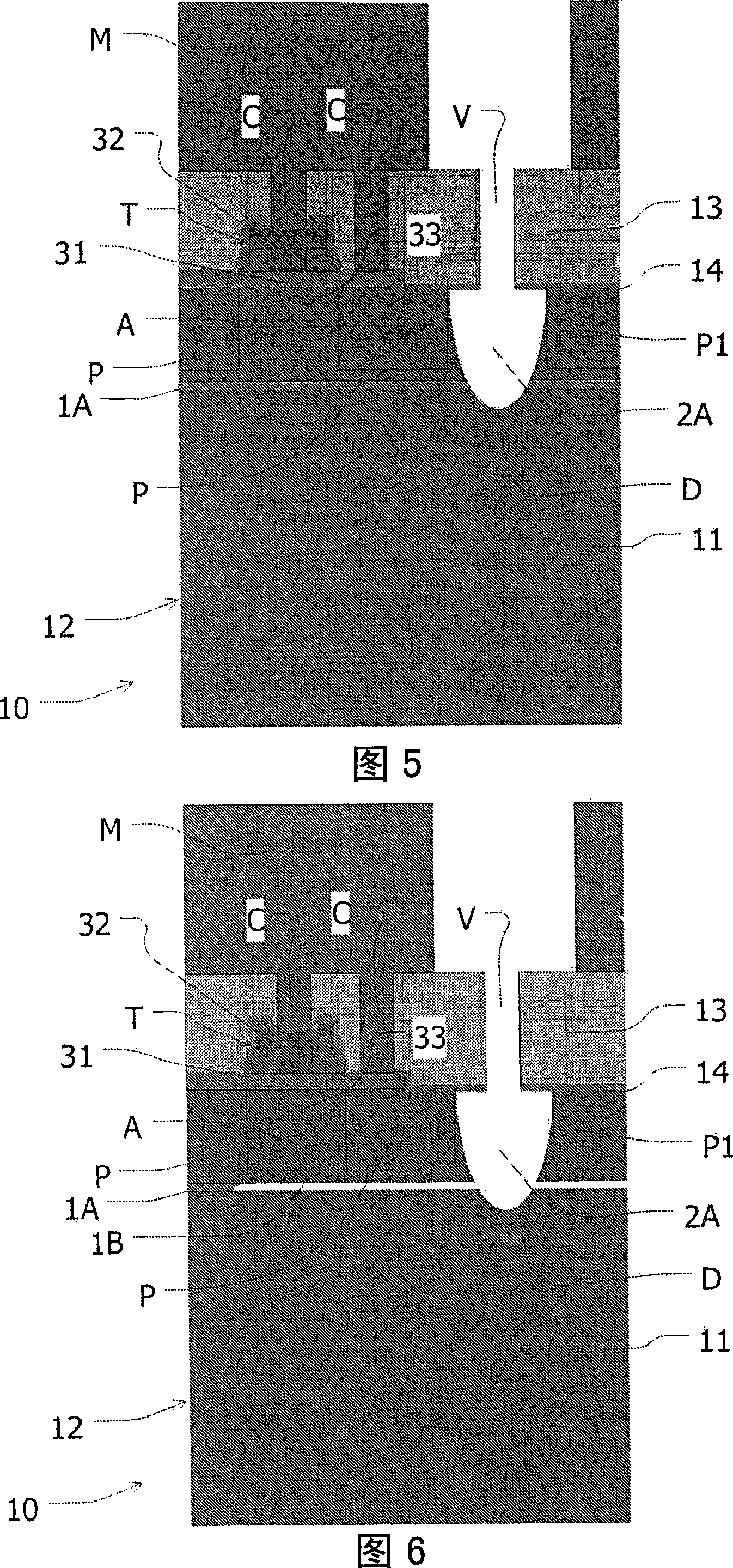
[0029] The figures are not drawn to scale and some dimensions are exaggerated for clarity. Wherever possible, similar regions or parts are indicated by the same numerals.

[0030] Figures 1 to 7 is a schematic cross-sectional view perpendicular to the thickness direction of a first example of a device according to the invention, showing successive stages of manufacture by the method according to the invention. The substantially complete device 10 of this example (see Figure 7 ) comprises a silicon semiconductor body 12 comprising a p-type silicon substrate 11 with a semiconductor layer structure arranged thereon and a bipolar transistor T. The transistor T, which in this example is a discrete transistor, is of the differential or epitaxial type, i.e. the base region 31 comprises a layered region grown on a semiconductor body which is polycrystalline on the passive region P and comprises the transistor A single crystal within the active region A of the collector region 33 ....


PUM


Abstract

The invention relates to a semiconductor device (10) with a substrate (11) and a semiconductor body (12) of silicon which comprises an active region (A) with a transistor (T) and a passive region (P) surrounding the active region (A) and which is provided with a buried conducting region (1) of a metallic material that is connected to a conductive region (2) of a metallic material sunken from the surface of the semiconductor body (12), by which the buried conductive region (1) is made electrically connectable at the surface of the semiconductor body (12). According to the invention, the buriedconducting region (1) is made at the location of the active region (A) of the semiconductor body (12). In this way, a very low buried resistance can be locally created in the active region (A) in thesemiconductor body (12), using a metallic material that has completely different crystallographic properties from the surrounding silicon. This is made possible by using a method according to the invention. Such a buried low resistance offers substantial advantages both for a bipolar transistor and for a MOS transistor.

Description

technical field [0001] The invention relates to a semiconductor device having a substrate and a silicon semiconductor body comprising an active area with transistors and an inactive area surrounding the active area and configured with a A buried conductive region of metallic material connected to a conductive region of metallic material. The term metallic material as used herein should be understood to mean a metal having a specific resistance comparable to technical resistance, for example, a metal, alloy, or compound such as copper, aluminum, tungsten, titanium, titanium nitride, or the like. The invention also relates to a method of manufacturing such a device. Background technique [0002] Such devices and methods are known from US patent US / 2005 / 0023617. Said document describes a semiconductor component having MOS transistors which form part of a memory and which are formed in the active region of a semiconductor body. The active region is surrounded by an inactive r...

Claims


Application Information

Patent Timeline
Patent Type & Authority Patents(China)
IPC IPC(8): H01L29/732H01L29/78H01L29/165H01L29/10H01L29/41H01L21/331H01L21/336H01L29/74H01L21/762H01L21/74
CPCH01L31/035236H01L29/78645Y02E10/50H01L29/42384H01L29/78696B82Y20/00H01L31/1812H01L21/743H01L21/76229H01L21/8222H01L21/8249H01L29/1087H01L29/41708H01L29/66242H01L29/7378H01L29/78
Inventor 韦伯·D·范诺尔特简·雄斯基菲利浦·默尼耶-贝拉德埃尔温·海曾
Owner NXP BV
Why Eureka
Try Eureka