Photoresist removeing method

A photoresist and wet removal technology, which is applied in photosensitive material processing, electrical components, semiconductor/solid-state device manufacturing, etc., can solve the problems of improper control of plasma ashing energy, silicon loss, and difficulty in completely removing photoresist and Surface and other problems to ensure performance, avoid serious depressions, and prevent excessive loss of silicon

Active Publication Date: 2008-07-02
SEMICON MFG INT (SHANGHAI) CORP +1
View PDF1 Cites 14 Cited by
  • Summary
  • Abstract
  • Description
  • Claims
  • Application Information

AI Technical Summary

Problems solved by technology

But when the feature size of the device enters the process node below 65nm, the gate oxide layer becomes thinner and thinner
If the plasma ashing energy is not properly controlled, or the SPM cleaning time is not properly controlled, it is very easy to damage the gate oxide layer, and then continue to corrode the silicon in the substrate 100, resulting in the loss of silicon, resulting in the appearance of the surface of the substrate 100 as Figure 4 Boom Depression 105 shown
If the plasma ashing process is not used, and the hard surface layer 150 and photoresist 130 are simply removed by wet cleaning, although the chance of damage to the gate oxide layer can be reduced, when the ion implantation energy is high, the hard surface layer 150 and the photoresist 130 formed When the surface layer 150 is thick, it is difficult to completely remove the photoresist and hard surface layer by simple wet cleaning (all wet strip), thus leaving such as Figure 5 Photoresist residues 133 and 134 are shown

Method used


Image

  • Photoresist removeing method
  • Photoresist removeing method
  • Photoresist removeing method

Examples


Embodiment Construction

[0019] In order to make the above objects, features and advantages of the present invention more comprehensible, specific implementations of the present invention will be described in detail below in conjunction with the accompanying drawings.

[0020] In the following description, numerous specific details are set forth in order to provide a thorough understanding of the present invention. However, the present invention can be implemented in many ways other than those described here, and those skilled in the art can make similar extensions without departing from the connotation of the present invention. Accordingly, the invention is not limited to the specific implementations disclosed below.

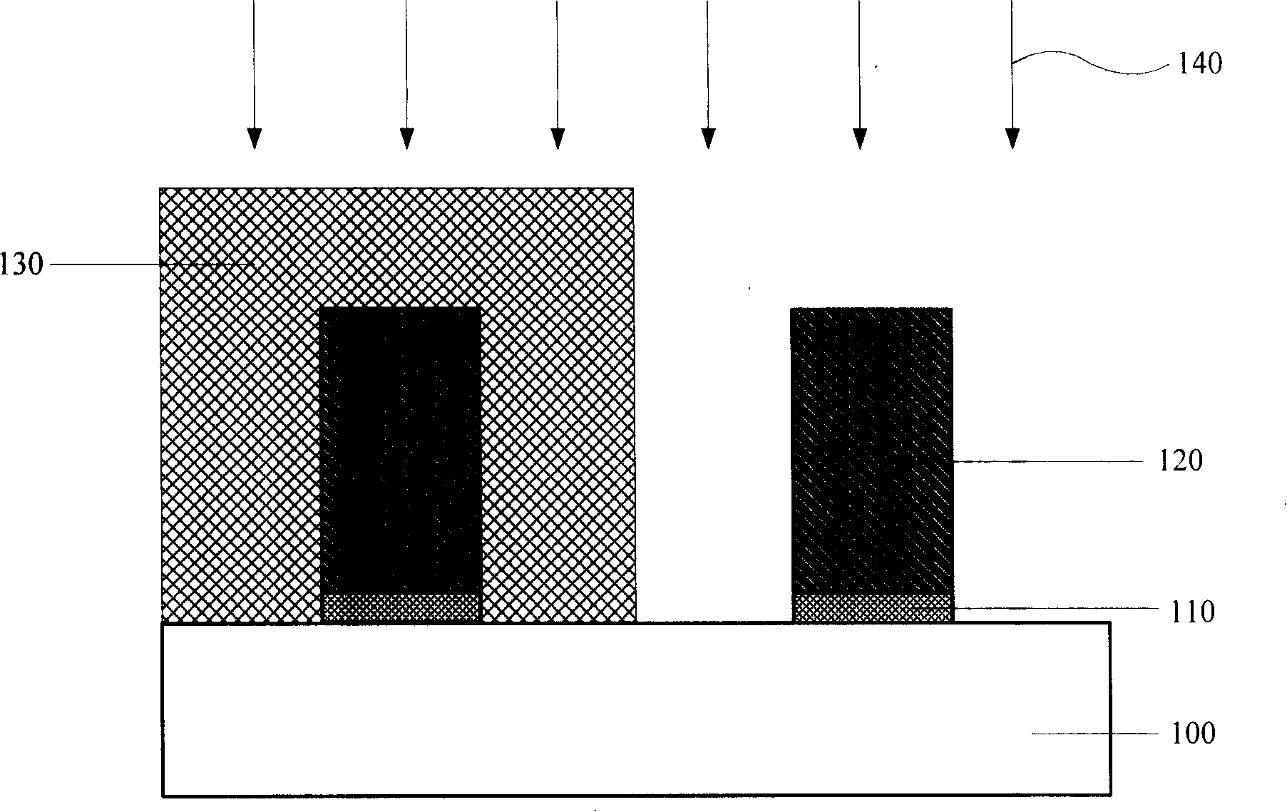
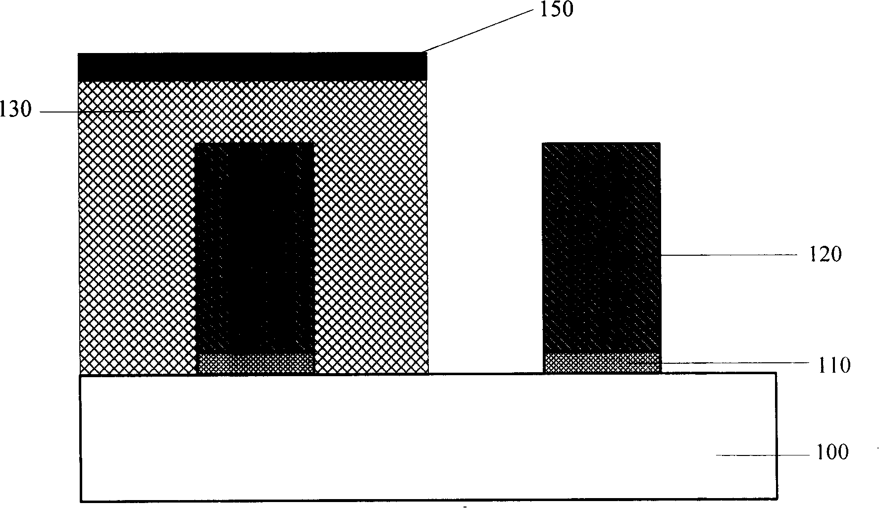
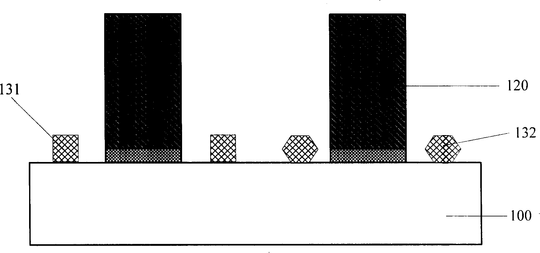
[0021] The method of the invention relates to the removal of the photoresist mask after ion implantation using the photoresist as the mask in the manufacturing process of the CMOS device. Figure 6 to Figure 8 To illustrate the device cross-sectional schematic diagram of the photoresi...


PUM


Abstract

The invention discloses a photoresist removal method, which comprises the methods of partial ashing and wet cleaning, i.e. removing a hard surface layer generated on the surface of a photoresist during the ion implantation process through plasma ashing technique, and cleaning the photoresist with SOM cleaning agent. The method can completely remove the photoresist, and can effectively prevent great loss of silicon on the substrate surface and avoid the appearance of severe sag, so as to ensure the performance of CMOS devices.

Description

technical field [0001] The invention relates to the technical field of semiconductor manufacturing, in particular to a method for removing a photoresist mask after ion implantation. Background technique [0002] With the rapid development of semiconductor manufacturing technology, in order to achieve faster computing speed, larger data storage capacity and more functions of semiconductor devices, semiconductor wafers are developing towards higher component density and high integration. The characteristics of CMOS devices Dimensions have entered the deep sub-micron stage, gate lengths have become thinner and shorter than ever. In order to avoid the short channel effect, a method of lightly doping the source region and the drain region, usually called extended doping, is currently used to form the lightly doped region of the NMOS device and the lightly doped region of the PMOS device. For NMOS devices, the doped n-type impurity ions are phosphorus (P + ) or arsenic (As); for...

Claims


Application Information

Patent Timeline
Patent Type & Authority Applications(China)
IPC IPC(8): G03F7/36G03F7/42G03F7/26
Inventor 郭佳衢刘焕新
Owner SEMICON MFG INT (SHANGHAI) CORP
Why Eureka
Try Eureka