LCD device array substrate, its defect mending method

A technology of liquid crystal display devices and array substrates, applied in transistors, optics, instruments, etc., can solve problems such as complex process, inability to repair lines while realizing line defects and point defects, failure to achieve normal pixel display quality, etc., to achieve a good display state Effect

Active Publication Date: 2008-07-09
KUSN INFOVISION OPTOELECTRONICS
View PDF0 Cites 36 Cited by
  • Summary
  • Abstract
  • Description
  • Claims
  • Application Information

AI Technical Summary

Problems solved by technology

The disadvantage of this technology is that if point defects and line defects occur at the same time, repair lines must be set up separately, and the process is more complicated
[0008] To sum up, the repair of pixel defects in the prior art is not a complete repair, so there is still a difference between the repaired pixel and the normal pixel, and there is a ce

Method used


Image

  • LCD device array substrate, its defect mending method
  • LCD device array substrate, its defect mending method
  • LCD device array substrate, its defect mending method

Examples


Embodiment 1

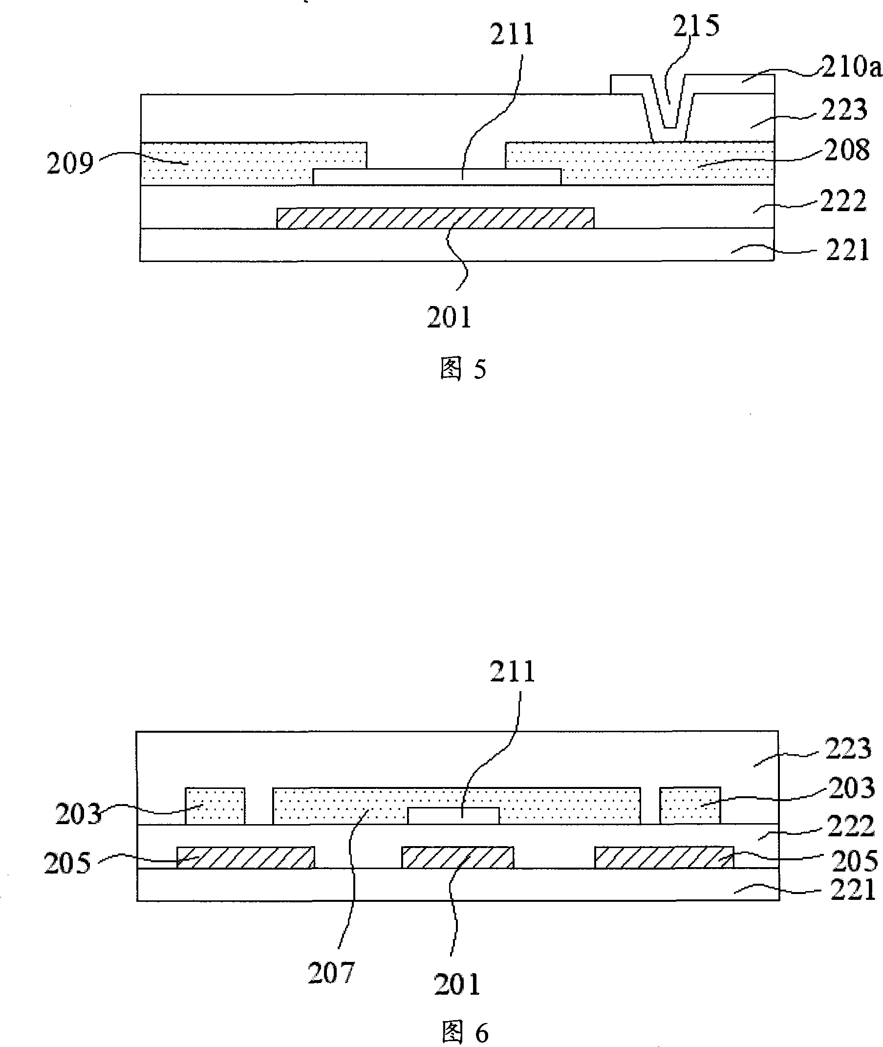
[0059] In the structure described below in this embodiment, both line defects and point defects can be repaired. The structure and repair method of the array substrate of the liquid crystal display device in this embodiment will be described with reference to FIGS. 4 to 9 .

[0060] FIG. 4 is a schematic diagram of a partial structure of an array substrate of a liquid crystal display device in this embodiment. Referring to Figure 4, 203 is a data line, 201 is a gate line, the data line 203 and the gate line 201 are respectively arranged in the data line layer and the gate line layer, and a plurality of data lines and a plurality of gate lines are intersected to define There are a plurality of pixel areas, and TFTs and pixel electrodes are provided in each pixel area. In order to more significantly represent the structural features of the present invention, only the TFT 213 located at the intersection position and the TFTs located above the gate line 201 and respectively are sh...

Embodiment 2

[0074] In the structure described below in this embodiment, both line defects and point defects can be repaired. The structure and repair method of the array substrate of the liquid crystal display device in this embodiment will be described with reference to FIGS. 10 to 15 .

[0075] FIG. 10 is a schematic diagram of a partial structure of an array substrate of a liquid crystal display device in this embodiment. The characteristic of the structure of this embodiment is that a second active region is provided, which can form a new thin film transistor when the original thin film transistor fails, so as to achieve the purpose of independently repairing point defects. Line defects on data lines.

[0076] Referring to Figure 10, 303 is a data line, 301 is a gate line, the data line 303 and the gate line 301 are respectively arranged in the data line layer and the gate line layer, and the intersection of multiple data lines and multiple gate lines is limited There are a pluralit...

Embodiment 3

[0091] The above-mentioned first repairing line is not limited to the structures disclosed in the above embodiments, as long as it partially overlaps with the data line and the second repairing line at the same time, the function of repairing the disconnection defect and point defect of the data line at the intersection position can be realized. Hereinafter, this embodiment will describe the structure and repair method of the above-mentioned array substrate of the liquid crystal display device with reference to FIG. 16 and FIG. 17 .

[0092] FIG. 16 is a schematic diagram of a partial structure of an array substrate of a liquid crystal display device in this embodiment. As shown in Figure 16, 403 is a data line, 401 is a gate line, the data line 403 and the gate line 401 are arranged in the data line layer and the gate line layer respectively, and a plurality of data lines and a plurality of gate lines are intersected to define A plurality of pixel areas, each of which is prov...


PUM


Abstract

The invention discloses an LCD device array substrate, which comprises a plurality of gate lines; a plurality of data lines intersecting the plurality of gate lines to define a plurality of pixel regions; pixel electrodes positioned in the pixel regions; gate line layers and data line layers, wherein, the plurality of gate lines and the plurality of data lines are respectively arranged; and a TFT including a source region, a gate, a source and a drain, wherein the gate, the source and the drain are respectively electrically connected with the gate lines, the data lines and the pixel electrodes. The invention also discloses a dot and/or line defect repair method of the LCD device array substrate. A new TFT formed by the repair method of the invention can be used for substituting for a TFT with pixel failure, thus achieving complete repair of dot defect of the array substrate and achieving better display state of the array substrate. The repair method can be also be used for repairing all structures with broken data lines, short-circuit and open-circuit at intersection portions of the data lines and the gate lines as well as dot defects.

Description

technical field [0001] The present invention relates to a liquid crystal display device, more specifically to an array substrate of a liquid crystal display device capable of repairing point defects and / or line defects and a repairing method thereof. Background technique [0002] As a kind of flat panel display, liquid crystal display has been widely used in various fields. Generally, a liquid crystal display has two substrates containing electrodes for generating an electric field, and a liquid crystal layer disposed between the two substrates, and controls the transmission of incident light by controlling the electric field intensity applied to the liquid crystal layer through the electrodes on the two substrates rate, so as to realize the control of the brightness and darkness of the display panel. [0003] FIG. 1 is a schematic diagram of the overall structure of an array substrate of a typical liquid crystal display device. Referring to Fig. 1, a plurality of gate lin...

Claims


Application Information

Patent Timeline
IPC IPC(8): G02F1/1362G02F1/13H01L29/786H01L27/12
Inventor 朱庆华乔艳冰朱健
Owner KUSN INFOVISION OPTOELECTRONICS
Why Eureka
Try Eureka