Package structure membrane of flip chip package

A technology of film-on-chip and liquid crystal display, which is applied in the direction of electrical components, electric solid devices, circuits, etc., and can solve problems affecting layout space configuration and other issues

Active Publication Date: 2008-07-09
AU OPTRONICS CORP
View PDF1 Cites 9 Cited by
  • Summary
  • Abstract
  • Description
  • Claims
  • Application Information

AI Technical Summary

Problems solved by technology

When testing the connection reliability of the tape-and-reel packaging structure, a test area must be generated for the part of the output pad extending beyond the cutting line, which affects the spatial configuration of the layout

Method used


Image

  • Package structure membrane of flip chip package
  • Package structure membrane of flip chip package
  • Package structure membrane of flip chip package

Examples


Embodiment Construction

[0027] The following will clearly illustrate the spirit of the present invention with the accompanying drawings and detailed descriptions. After any person skilled in the art understands the preferred embodiments of the present invention, they can be changed and modified by the technology disclosed in the present invention without departing from the present invention. spirit and scope.

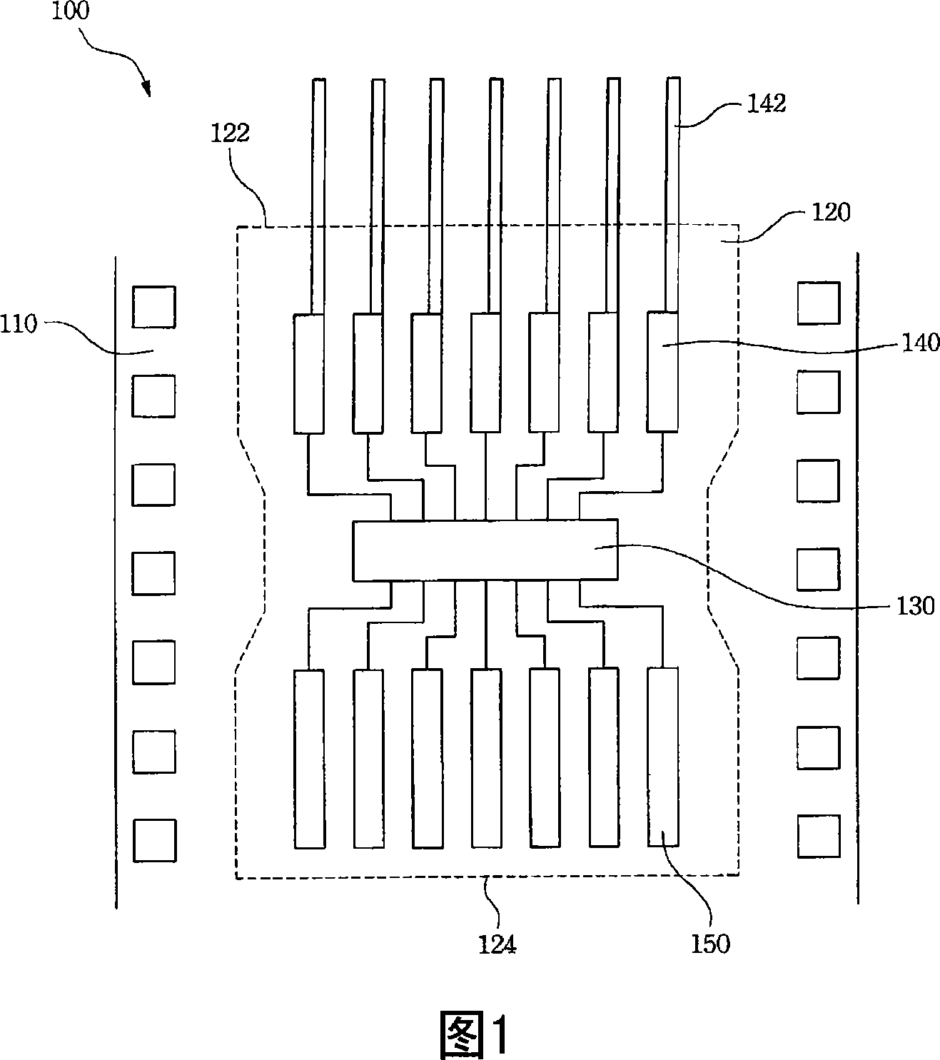
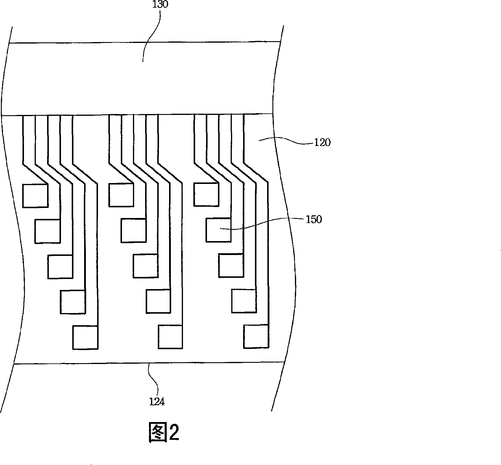
[0028] Referring to FIG. 1 , it is a schematic diagram of a preferred embodiment of the chip-on-film packaging structure of the present invention. The chip-on-film structure 100 (Chip On Film; COF) can be applied in a liquid crystal display, including a substrate 120, a driver chip 130 disposed on the substrate 120, and a plurality of input pads 140 and output pads disposed on the substrate 120. Pad 150. The driver chip 130 is electrically connected to the input pad 140 and the output pad 150 respectively, which can be achieved through, for example, a metal bump (bump) (not shown in the figur...


PUM


Abstract

The invention provides a thin film flip chip packaging structure, which can be applied in a liquid crystal display; the invention comprises a substrate, a drive chip which is arranged on the substrate and a plurality of input pads and output pads. The substrate is provided with a first cutting edge and a second cutting edge. The input pads which are arranged on the substrate are electrically connected with the drive chip, and the input pads are extended with extension parts to the first cutting edge. The width of the extension parts are as small as possible to reduce the sputtering of metal particles and the first cutting edge can cut through the extension parts. The output pads which are arranged on the substrate are electrically connected with the drive chip, wherein, the output pads are positioned between the drive chip and the second cutting edge. The invention can effectively avoid the case of the sputtering of the metal particles when cutting the thin film flip chip structure by using a rolling strip.

Description

technical field [0001] The invention relates to a film-on-chip packaging structure, and in particular to a film-on-chip packaging structure of a driving chip of a liquid crystal display. Background technique [0002] Liquid crystal display has rapidly grown into the mainstream of the display market due to its advantages of thinness, lightness, small size and power saving. The image presentation of the liquid crystal display panel is to transmit signals through an external driver chip, and then control the arrangement and direction of the liquid crystal on the panel to achieve image quality. display purpose. [0003] The driving method of the display panel traditionally separates two flexible printed circuit boards with a data driver chip and a scan driver chip separately packaged with a tape automatic bonding method (TapeAutomated Bonding; TAB) respectively. The data lines and scan lines of the display panel are connected to drive multiple pixels of the display panel. Howe...

Claims


Application Information

Patent Timeline
IPC IPC(8): H01L23/498
Inventor 张格致杨智翔许胜凯黄益志陈滢照
Owner AU OPTRONICS CORP
Why Eureka
Try Eureka