Display panel

A display panel and substrate technology, applied in nonlinear optics, instruments, optics, etc., can solve problems affecting image quality, long exposure time, liquid crystal layer contamination, etc.

Inactive Publication Date: 2008-07-16
AU OPTRONICS CORP
View PDF0 Cites 10 Cited by
  • Summary
  • Abstract
  • Description
  • Claims
  • Application Information

AI Technical Summary

Problems solved by technology

[0004] However, when curing the photosensitive colloid, if the light energy provided is too small, the exposure time is too short, or because the wire structure on the substrate blocks part of the light, the photosensitive colloid cannot be cured smoothly, so that the liquid crystal molecules in the liquid crystal layer In contact with the uncured photosensitive colloid, impurities or solvents in the colloid penetrate into the liquid crystal layer, causing the liquid crystal layer to be polluted and affecting the image quality, or during the curing process, the exposure time is too long, so that the liquid crystal molecules in the liquid crystal layer Exposure to light for a long time will degrade the liquid crystal molecules, which will also lead to the occurrence of bad lines (mura) in the development process

Method used


Image

  • Display panel
  • Display panel
  • Display panel

Examples


no. 1 example

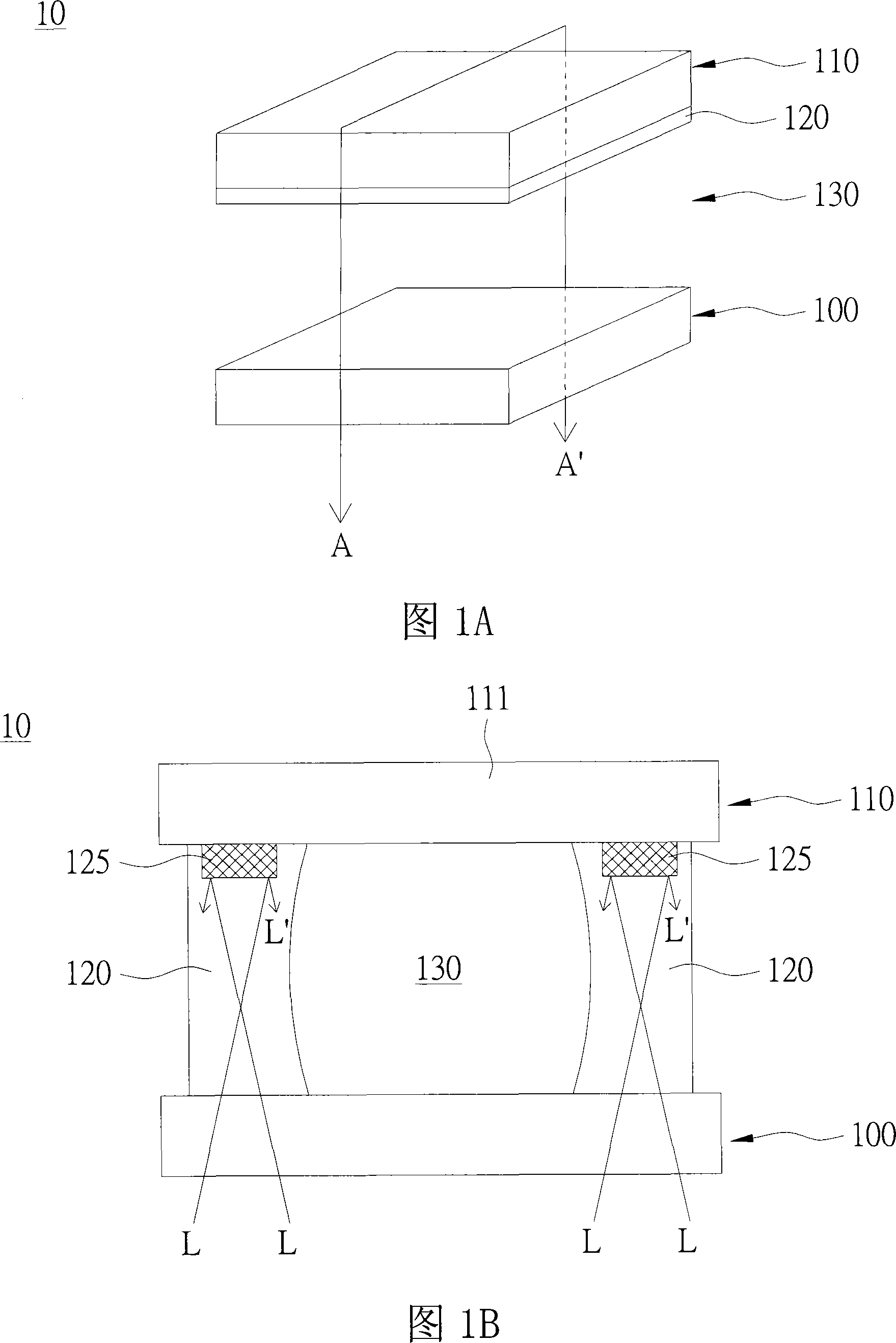
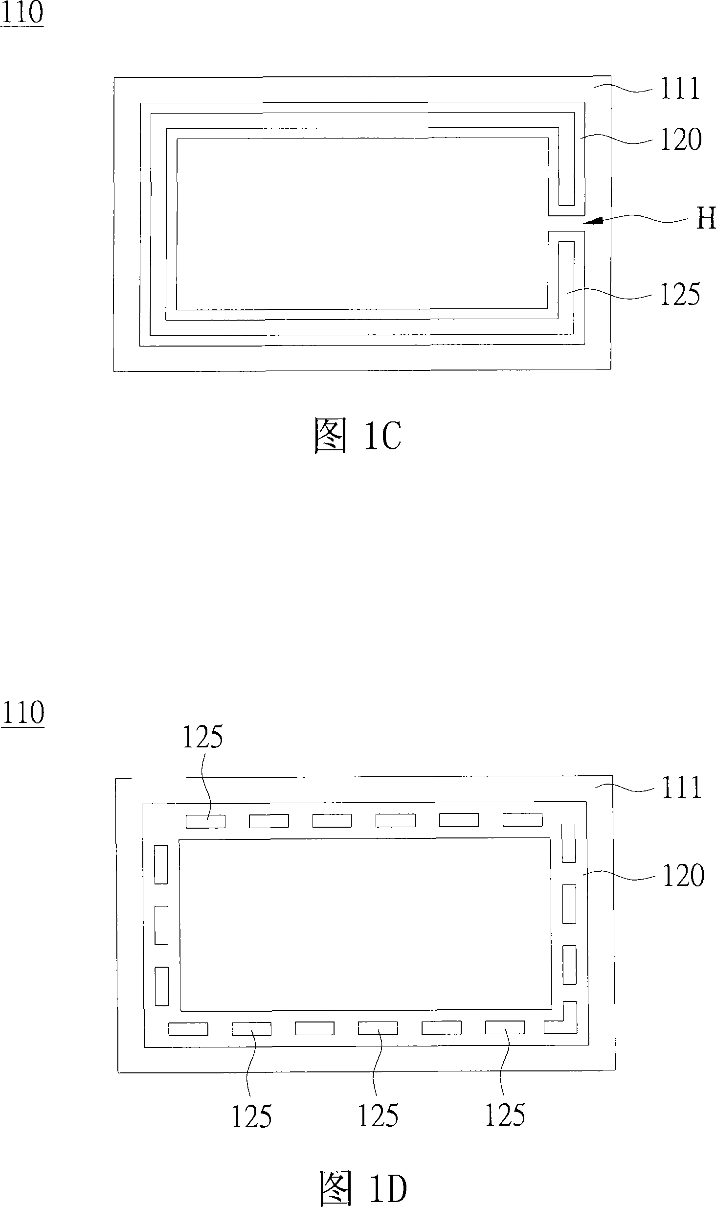
[0053] FIG. 2 is a cross-sectional view of a display panel according to a first embodiment of the present invention. As shown in FIG. 2 , the display panel 20 includes a color filter substrate 210 , an active array substrate 200 and a liquid crystal layer 230 therebetween. The display panel 20 has a display area T and a bonding area C, and the display area T is surrounded by the bonding area C along its periphery.

[0054] The color filter substrate 210 includes a base 211, and the light-shielding layers 212a and 212b are located on the base 211. In the display area T, the color filter layers R, G, and B are located on the base 211, which can partially cover the light-shielding layer 212a, and are insulated. The layer 223 covers the light-shielding layer 212a and the color filter layers R, G, and B. The material of the insulating layer 223 is, for example, an organic material. The common electrode 224 is located on the insulating layer 223. The reflective structure 225 include...

no. 2 example

[0059] FIG. 3 is a cross-sectional view of a display panel according to a second embodiment of the present invention. As shown in FIG. 3 , the difference from the first embodiment is that the reflective structure 325 is located on the active array substrate 300 , and the rest of the components are substantially the same, and will not be repeated here. When the process of curing the photosensitive sealant 320 is performed, the light L is provided from the side of the color filter substrate 310 into the photosensitive sealant 320, and then reflected by the reflective structure 325 to form the light L', which enters the light again. The sensitive sealing glue 320 is used to cure the photosensitive sealing glue 320 .

no. 3 example

[0061] FIG. 4 is a cross-sectional view of a display panel according to a third embodiment of the present invention. As shown in FIG. 4 , the liquid crystal panel 40 includes a color filter on an active array substrate (color filter on array, COA) 400 , an opposite substrate 410 and a liquid crystal layer 430 therebetween. The difference from the first embodiment is that the liquid crystal panel 40 uses color filters on the active array upper substrate 400 , so the opposite substrate 410 does not need a color filter layer. In the color filter active array upper substrate 400 , the light-shielding layer 412 b and the color light layers R, G, and B are located on the insulating layer 403 . The manufacturing process of the reflective structure 425 can directly form the first adjustment structure 425 a , the second adjustment structure 425 b and the reflective layer 425 c on the substrate 411 , or form the metal reflective structure on the substrate 411 . The rest of the compon...


PUM

PropertyMeasurementUnit
reflectanceaaaaaaaaaa

Abstract

The invention discloses a display panel, comprising a first substrate which comprises a first base plate and a reflection structure positioned on the first base plate, a second substrate and a photosensitive seal adhesive which is arranged between the first substrate and the second substrate for connecting the first substrate and the second substrate, wherein the at least one reflection structure is positioned between the photosensitive seal adhesive and the first base plate. The invention mainly provides a display panel and a method for making the same in the process of solidification of photosensitive seal adhesives for increasing the utilization rate of light and reducing the needed light ray energy.

Description

technical field [0001] The invention relates to a display panel. The display panel has a photosensitive sealing adhesive and a reflective structure. The reflective structure is used to reflect the light used to cure the photosensitive sealing adhesive, so as to reduce the amount of light required to cure the photosensitive sealing adhesive. light energy. Background technique [0002] Flat panel displays have been widely used because of their thinness, shortness and low radiation characteristics. Currently widely used liquid crystal displays usually have two substrates with a liquid crystal layer interposed therebetween. A sealing glue is located between the two substrates to bond the two substrates and hermetically seal the liquid crystal layer between the two substrates. [0003] Generally speaking, thermosetting or photosensitive colloids are used for sealing glue. In the manufacturing process of liquid crystal display panels, after coating colloid on one of the substrat...

Claims


Application Information

Patent Timeline
Patent Type & Authority Applications(China)
IPC IPC(8): G02F1/1335G02F1/1333
Inventor 沈益民黄于容
Owner AU OPTRONICS CORP
Why Eureka
Try Eureka