Package structure of semiconductor device

A device packaging and semiconductor technology, which is applied in semiconductor devices, semiconductor/solid-state device components, electric solid-state devices, etc., can solve the problems of low power density, limiting the power of packaged chips, and poor heat dissipation effect of components

Active Publication Date: 2008-07-30
JINAN JINGHENG ELECTRONICS
View PDF0 Cites 4 Cited by
  • Summary
  • Abstract
  • Description
  • Claims
  • Application Information

AI Technical Summary

Problems solved by technology

At present, the packaging size of semiconductor devices is getting smaller and smaller. The existing packaging forms are affected by the plastic encapsulant and lead frame, the heat dissipation effect of components is poor, and the power density is low, which limits the power of the packaged chip.

Method used


Image

  • Package structure of semiconductor device
  • Package structure of semiconductor device

Examples


Embodiment 1

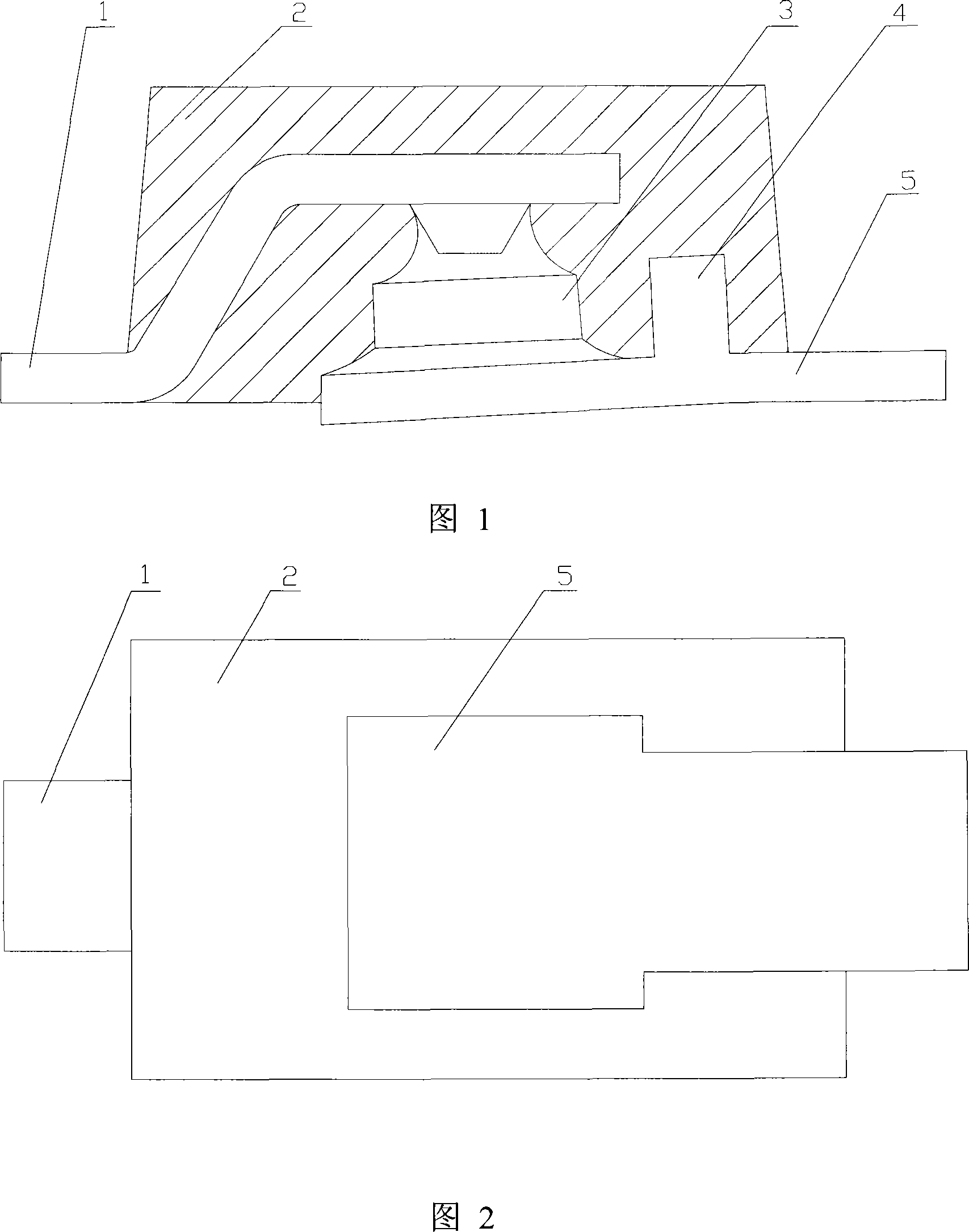
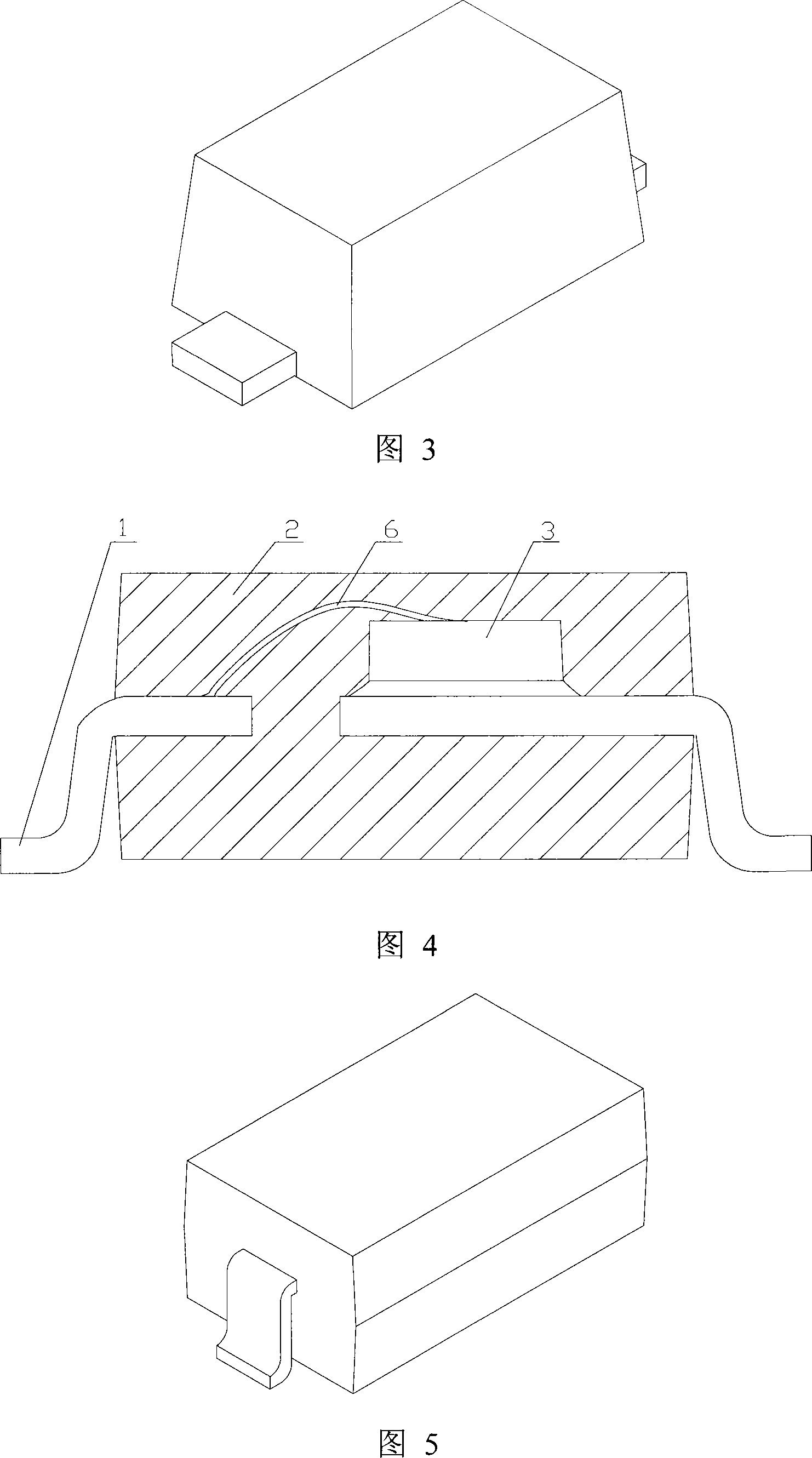
[0024] Referring to accompanying drawings 1 to 3 of the description, the semiconductor device packaging structure of the present invention is an improvement of the lead frame semiconductor device packaging structure, and adopts the following technical solutions: the present invention also includes lead frames 1, 5 and wafers 3 electrically connected thereto, and an integrated Structure of the packaging case 2. The improvement is that the chip 3 is sandwiched between the lead frames 1 and 5 , wherein the lower surface of the lead frame 5 is exposed outside the package case 2 . This subverts the structural form of the original lead frame semiconductor packaging structure of the hermetic package, and is also different from the structural form of the external heat dissipation device. In the present invention, the lead frame 5 not only serves as the welding electrode of the chip 3, but also serves as a heat sink. The structure is compact, and at the same time, an intermediate heat ...

Embodiment 2

[0027] Compared with embodiment 1, in order to prevent flashing during the packaging process more effectively, the present embodiment adopts the scheme that the included angle between the lower surface of the lead frame 5 and the lower surface of the packaging case 2 is 5°, which is more Effectively prevent overflow.

[0028] It is also well known that the greater the angle between the lower surface of the lead frame 5 and the lower surface of the package case 2 , the less likely the encapsulation material will cover the lower surface of the lead frame 5 . At the same time, in order to consider the soldering installation of the semiconductor package, if the angle is too large, it will inevitably affect the cleanliness and stability of its soldering to the motherboard. It is more appropriate that the angle is less than 7°, preferably less than 5°. If it is too small, it cannot effectively prevent the encapsulation compound from covering the lower surface of the lead frame 5, a...

Embodiment 3

[0031] Referring to accompanying drawings 1 to 3 of the specification, compared to Embodiments 1 and 2, the packaging structure of the semiconductor device of the present invention is provided with bumps 4 on the lower surface of the lead frame 1, and the upper surface is exposed to the outside of the packaging casing 2, so that External forced cooling means can be introduced, which is suitable for the packaging of high-power devices.


PUM


Abstract

The invention relates to a semiconductor device package structure, in particular to a package structure of a miniature semiconductor device, which comprises lead frames and a wafer electrically connected with the lead frame, and integrated package housing. The wafer is sandwiched between the lead frames, and the lower surface of the lead frames below the chip is exposed to the outside of the package housing. The invention has the advantages of compact structure, low manufacture cost, good heat dissipation effect and effectively improved unit power density.

Description

(1) Technical field [0001] The invention relates to a package structure of a semiconductor device, in particular to a package structure of a small semiconductor device. (2) Background technology [0002] There are many packaging structures for semiconductor devices, from DIP, SOP, QFP, PGA, BGA to CSP and then to SIP, and the technical indicators are advanced from generation to generation. These are all developed by predecessors according to the assembly technology and market demand at that time. Overall, it has about three major innovations: the first was from pin-insert packaging to surface mount packaging in the 1980s, which greatly improved the assembly density on printed circuit boards; the second was in the In the 1990s, the ball-shaped rectangular package appeared, which not only met the demand for high pins in the market, but also greatly improved the performance of semiconductor devices. When it comes to small semiconductor devices, pin plug-in packages and surface...

Claims


Application Information

Patent Timeline
IPC IPC(8): H01L23/495H01L23/31H01L23/367
CPCH01L24/33H01L2224/32245H01L2224/48091H01L2224/48247H01L2224/73265H01L2924/181H01L2924/00014H01L2924/00H01L2924/00012
Inventor 孟博苏云荣
Owner JINAN JINGHENG ELECTRONICS
Why Eureka
Try Eureka