Method for interconnecting multilayer phase transition memory array and lower layer peripheral circuit
A technology of phase-change storage and peripheral circuits, applied in circuits, information storage, static memory, etc., can solve problems that are not conducive to low voltage and low power consumption of chips
- Summary
- Abstract
- Description
- Claims
- Application Information
AI Technical Summary
Problems solved by technology
Method used
Image

Examples
Embodiment 1
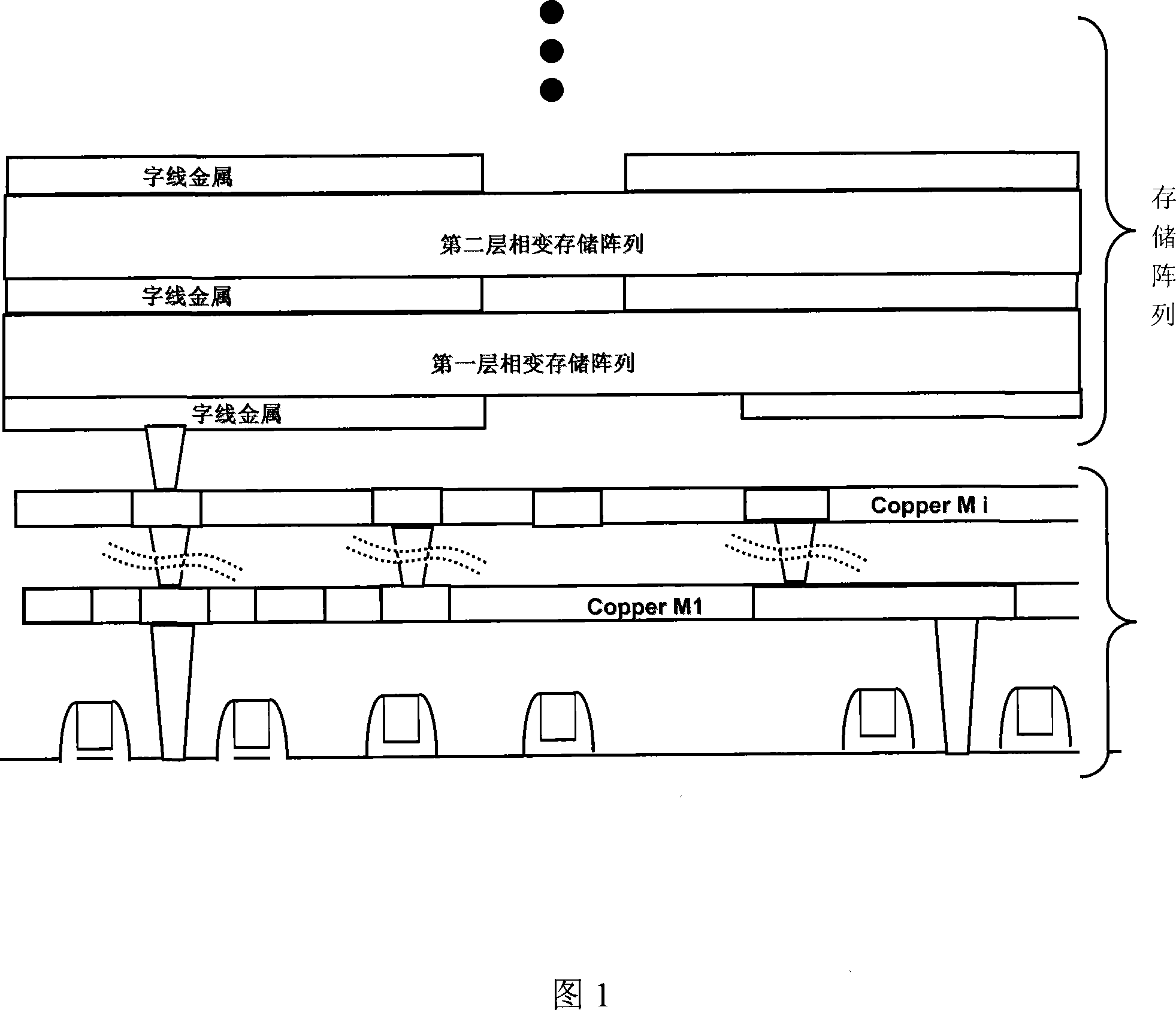
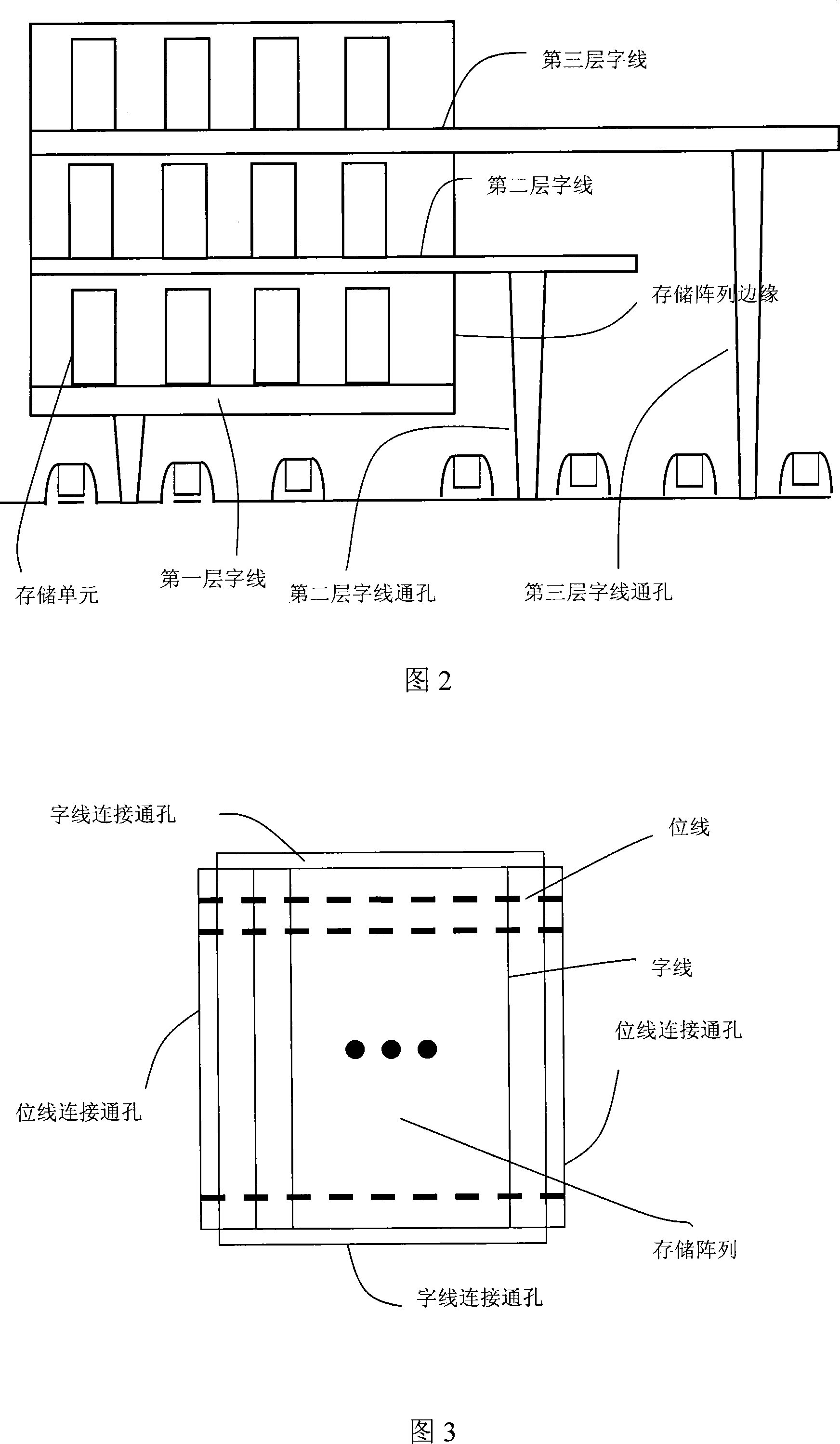
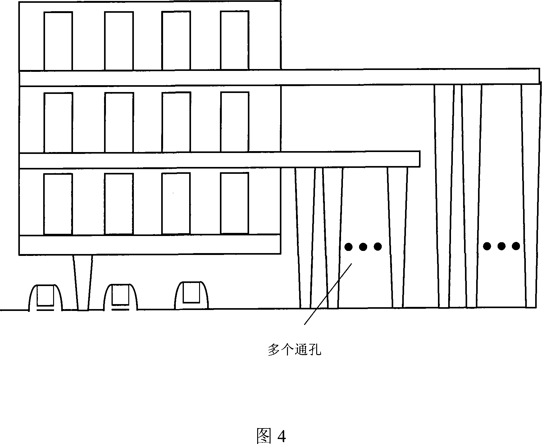
[0022] As shown in Figure 2, the storage units of each layer are aligned up and down. Except that the phase-change memory array of the first layer can be directly connected with the peripheral circuit of the bottom layer, all word (or bit) lines of the layers above the first layer are introduced into the peripheral circuit of the bottom layer through the through holes arranged at the edge of the memory array. Due to the relatively small area occupied by the through holes, the area of the limited number of through holes is almost negligible under a large-capacity memory chip. The top view of the overall layout is shown in Figure 3.
[0023] As a feasible optimization method, if the area requirement is not very strict, the series resistance of the vias can be reduced by increasing the number of vias. As shown in Figure 4, a plurality of through holes are added at the edge of the memory array.
[0024] In theory, this method can connect storage arrays of any level. However, ...
Embodiment 2
[0026] Leading out the word (or bit) line at the edge of the memory array will concentrate the bottom peripheral circuits on the edge of the memory array, which may cause difficulties in the design of the bottom circuit.
[0027] Another method proposed in this embodiment can prevent the interconnection lines from being concentrated on the edge of the storage array. The memory cells of the upper layer and the memory cells of the lower layer are staggered by a certain distance to allow a certain distance of through holes. As shown in FIG. 5 , the squares with thin solid lines represent the first layer memory cells, the squares with dashed lines represent the second layer memory cells, the small black holes in the squares represent through holes, and the rectangles with thick solid lines represent word line metals. Assume that the minimum side length of the memory cell is b, the minimum distance between the memory cells is m; the size of the through hole is a, and the minimum di...
Embodiment 3
[0031] There is a limit to the number of layers in the staggered arrangement of memory cells. In order to break through this limitation and at the same time facilitate the design of the underlying circuit, this embodiment proposes a method for sharing word lines by memory cells of different levels.
[0032] As shown in Figure 7, the memory cells of all levels are aligned, and the gap between the memory cells is used to drill through holes so that the word lines between the upper and lower layers are connected together. Since the bit lines of each memory cell between the upper and lower layers are not connected to each other, from the perspective of the peripheral circuit, it is equivalent to adding more memory cells on the word line. Within the allowable range of design rules, the area of the through hole will not affect the overall area of the memory array.
PUM
 Abstract
Description
Claims
Application Information
 - R&D
- Intellectual Property
- Life Sciences
- Materials
- Tech Scout
- Unparalleled Data Quality
- Higher Quality Content
- 60% Fewer Hallucinations
Browse by: Latest US Patents, China's latest patents, Technical Efficacy Thesaurus, Application Domain, Technology Topic, Popular Technical Reports.
© 2025 PatSnap. All rights reserved.Legal|Privacy policy|Modern Slavery Act Transparency Statement|Sitemap|About US| Contact US: help@patsnap.com