Grid making method

A manufacturing method and gate technology, applied in the field of gate manufacturing, can solve problems such as enhancement and incomplete etching, and achieve the effects of complete outline, improved reliability and product yield.

Inactive Publication Date: 2008-08-06
POWERCHIP SEMICON CORP
View PDF0 Cites 11 Cited by
  • Summary
  • Abstract
  • Description
  • Claims
  • Application Information

AI Technical Summary

Problems solved by technology

[0006] Another purpose of providing embodiments according to the present invention is to provide a gate manufacturing method, which can improve the problem of incomplete etching and improve the control of the gate profile in the process

Method used


Image

  • Grid making method
  • Grid making method
  • Grid making method

Examples


Embodiment Construction

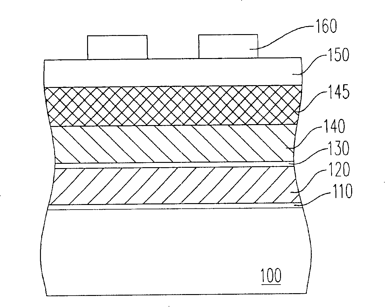
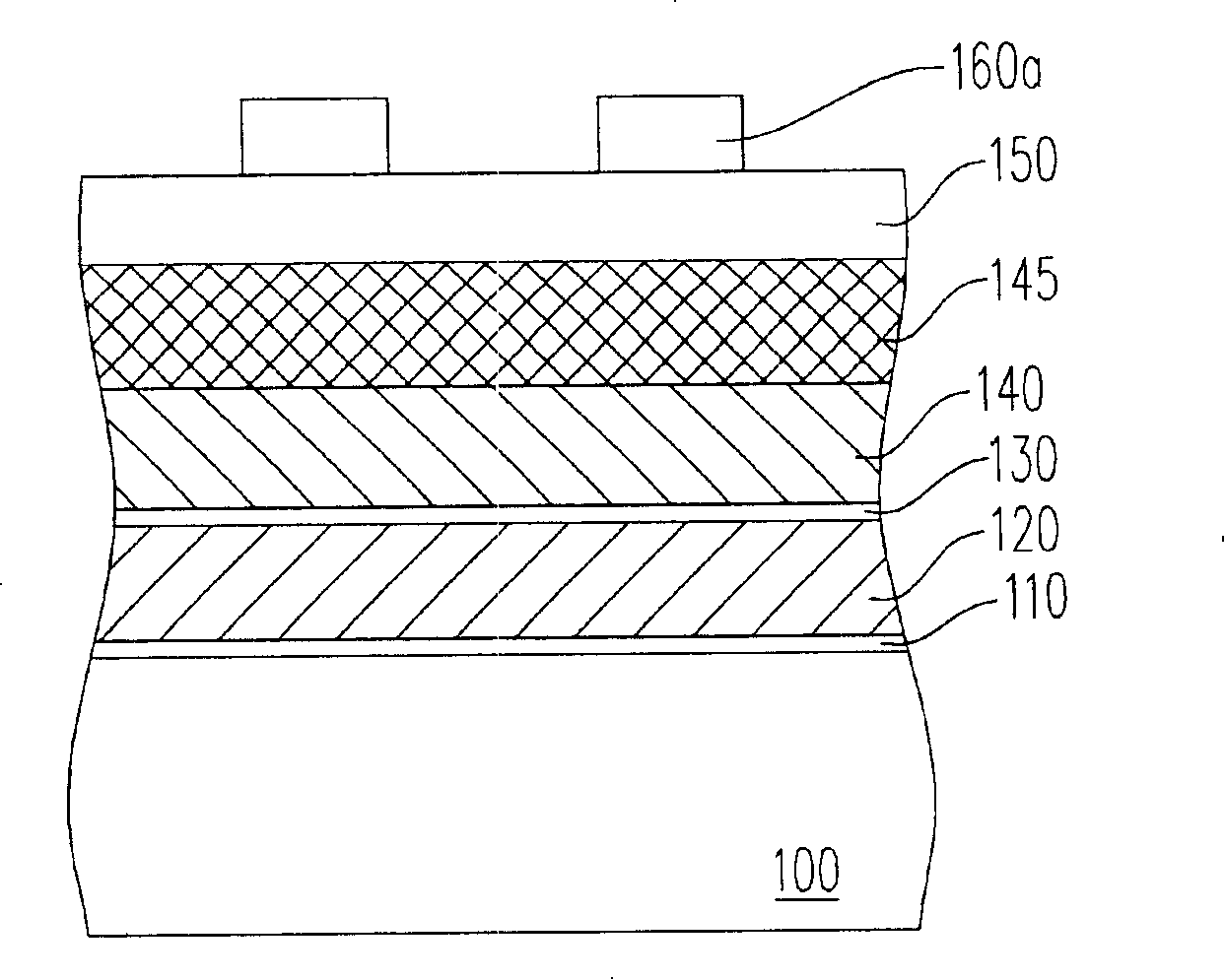
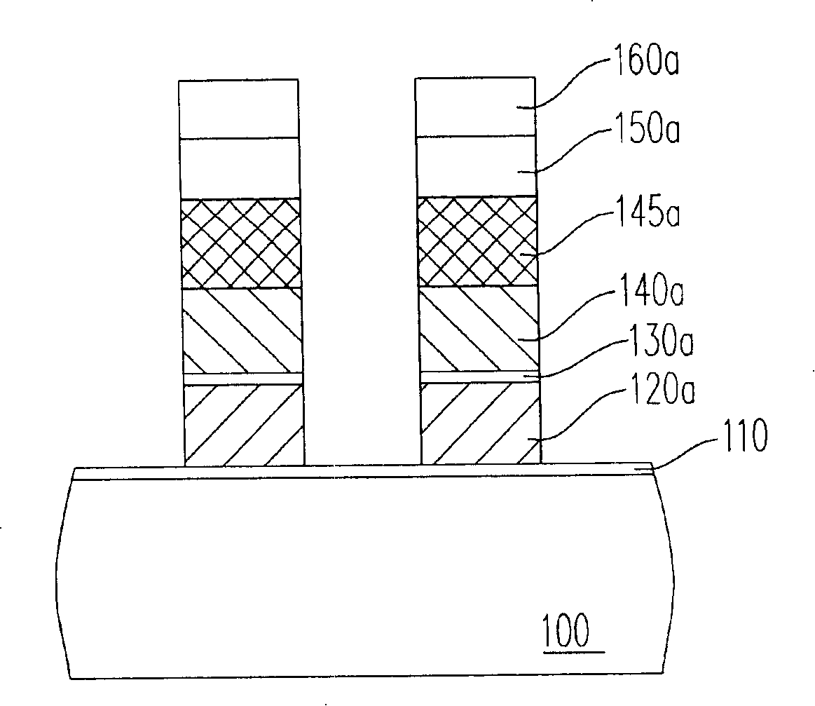
[0048] Figure 1A to Figure 1D It is a schematic cross-sectional view illustrating a manufacturing process of a gate according to an embodiment of the present invention.

[0049] Please refer to Figure 1A , the gate manufacturing method of this embodiment is applied in the manufacturing process of the memory element, of course, the present invention is not limited thereto. Firstly, a substrate 100 is provided, on which a tunnel dielectric layer 110 , a floating gate material layer 120 , an inter-gate dielectric layer 130 and a control gate material layer 140 have been sequentially formed.

[0050] Wherein, the material of the tunneling dielectric layer 110 is, for example, silicon oxide, and its formation method is, for example, thermal oxidation or chemical vapor deposition.

[0051] The material of the floating gate material layer 120 and the control gate material layer 140 is, for example, doped polysilicon, which is formed by, for example, using a chemical vapor depositi...


PUM


Abstract

The invention provides a manufacturing method for a grid electrode, including the following steps: a substrate is provided, at least one grid electrode material layer is formed on the substrate; a pattern mask layer is formed on the grid electrode material layer; the transverse size of the pattern mask layer is microcopied by the wet-type etching process; the pattern mask layer is taken as the mask to remove a part of the grid electrode material layer, thereby forming a grid electrode with a preset size.

Description

technical field [0001] The invention relates to a method for manufacturing a semiconductor structure, and in particular to a method for manufacturing a gate. Background technique [0002] With the vigorous development of integrated circuits and the strengthening of the functions of electronic products, the application circuits are becoming more and more complex. In order to effectively increase the operating speed of the entire circuit, the density of transistors required in the integrated circuit is also greatly increased. That is to say, the size of each element will continue to shrink, so that the number of transistors in a unit area can be increased. However, the size of components cannot be reduced indefinitely, and there are difficulties to be overcome in terms of design criteria, physical characteristics of components, and even process feasibility. [0003] Taking a metal oxide semiconductor transistor as an example, in the process of defining and shrinking the gate...

Claims


Application Information

Patent Timeline
Patent Type & Authority Applications(China)
IPC IPC(8): H01L21/28H01L21/308H01L21/336
Inventor 吴至宁王伟民萧国坤
Owner POWERCHIP SEMICON CORP
Why Eureka
Try Eureka