Packaging conductive structure and its manufacturing method

A technology of conductive structure and manufacturing method, which is applied in semiconductor/solid-state device manufacturing, circuits, electrical components, etc., and can solve the problems of semiconductor chip failure, bump 19 falling off, open circuit, etc.

Active Publication Date: 2008-08-20
CHIPMOS TECH INC
View PDF0 Cites 6 Cited by
  • Summary
  • Abstract
  • Description
  • Claims
  • Application Information

AI Technical Summary

Problems solved by technology

[0005] However, in the existing package conductive structure, the bonding buffer capability of the bump 19 on the UBM layer 17 has its limitations in terms of structure and material, and the conductive area of ​​the pad 13 has also been determined before packaging. Poor

Method used


Image

  • Packaging conductive structure and its manufacturing method
  • Packaging conductive structure and its manufacturing method
  • Packaging conductive structure and its manufacturing method

Examples


Embodiment Construction

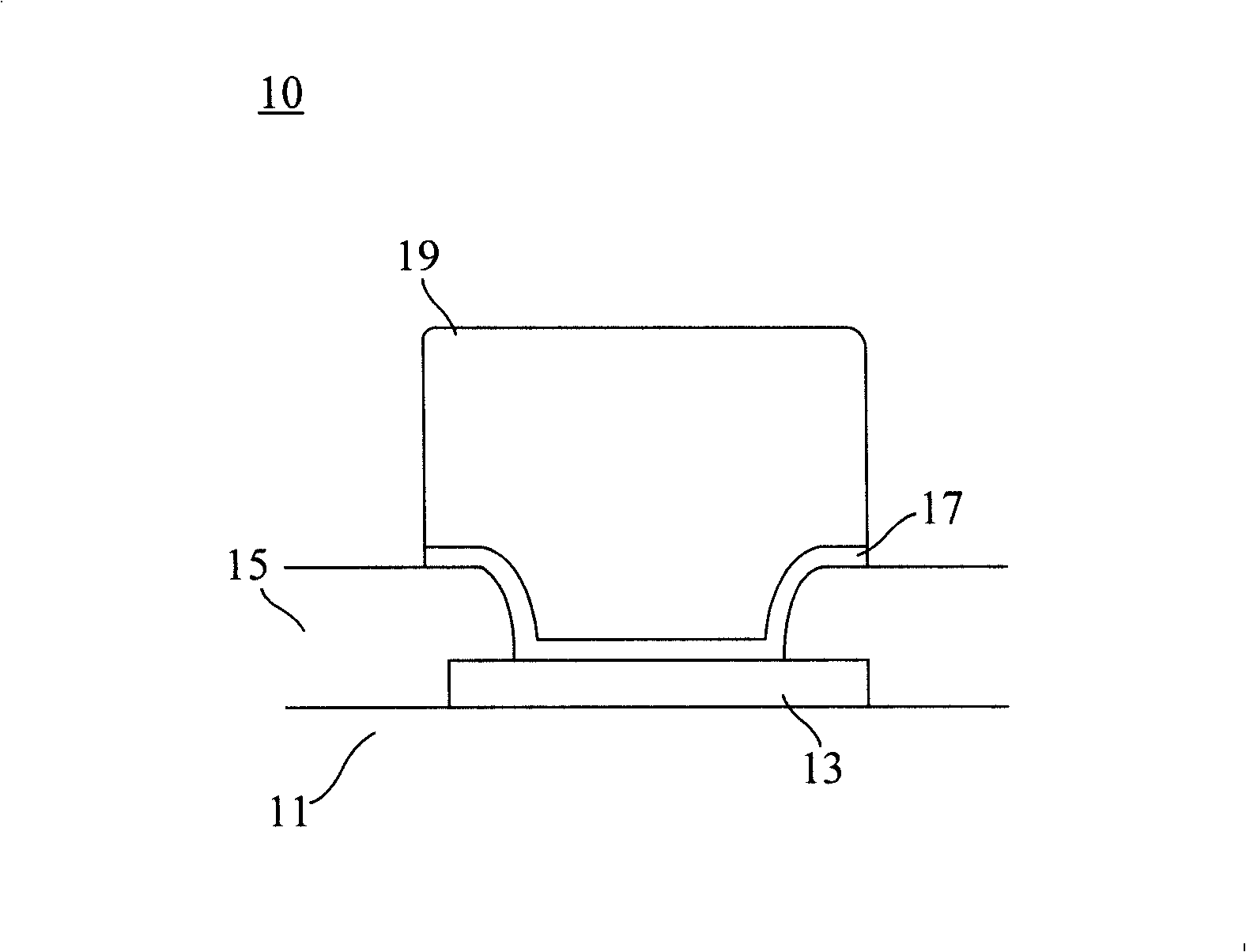
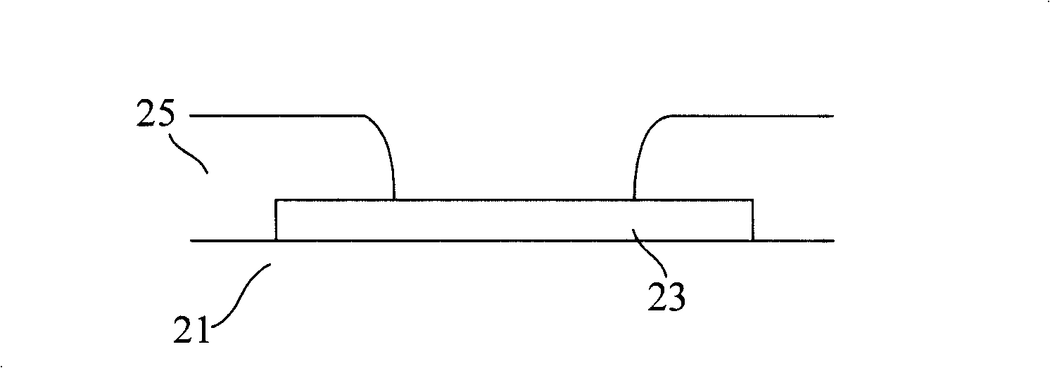
[0017] The invention discloses a packaging conductive structure for semiconductor substrates and its manufacturing method; first refer to figure 2 The semiconductor substrate 21 includes a pad 23 , which is generally made of aluminum, and serves as a contact point for the semiconductor structure inside the semiconductor substrate 21 to be electrically connected to the outside. Then, a protective layer 25 is formed on the semiconductor substrate 21, which partially covers the liner 23 to define an accommodating space; in actual manufacturing, a photoresist layer can be formed first, and then patterned. An etching process is used to remove part of the photoresist material to form an accommodating space and partially expose the liner 23 .

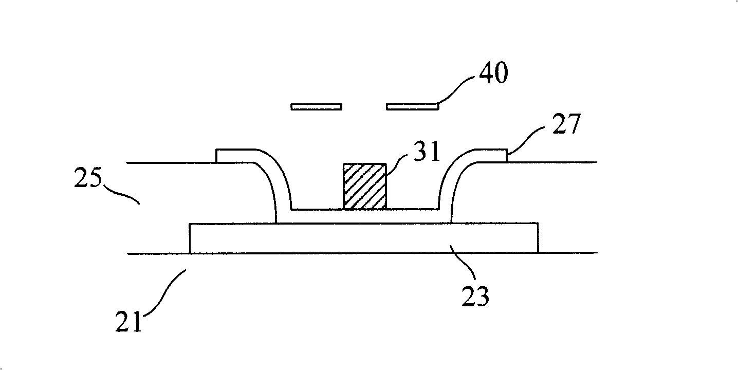
[0018] see further image 3 , forming an under bump metal layer (Under Bump Metal, UBM) 27 in the accommodation space, which is electrically connected to the pad 23 of the semiconductor substrate 21, wherein the under bump metal layer 27 is ...


PUM


Abstract

The invention relates to an encapsulated conducting structure for a semiconductor substrate and the forming method thereof. The encapsulated conducting structure consists of a under bump metal layer covering the liner of the semiconductor substrate, at least one auxiliary part is arranged on the under bump metal layer, and then a bump metal layer is covered, and finally a bump is arranged on a bump conducting layer. Thereby, the bump can electrically connect with the lining of the semiconductor substrate by the under bump metal layer and the bump conducting layer, and provide better connecting buffer capacity and conduction property.

Description

technical field [0001] The invention relates to a packaging conductive structure used for semiconductor substrates; in particular, a packaging conductive structure that can improve conductivity and bump joint buffering ability. Background technique [0002] Today's electronic products usually have semiconductor chips to provide control or logic operation functions. Due to the continuous improvement of process technology, semiconductor chips are becoming smaller and smaller, and the package size is gradually shrinking. [0003] The traditional electronic packaging technology that uses wire bonding to bond semiconductor chips to other components has long been insufficient. Instead, flip-chip bonding technology that uses bumps as chips to bond to other components has been replaced. More specifically, there are multiple bumps on the surface of the semiconductor chip, which are electrically connected to the internal structure of the chip and used to bond with other components. In...

Claims


Application Information

Patent Timeline
IPC IPC(8): H01L23/485H01L21/60
CPCH01L24/11H01L2224/11H01L2924/00012
Inventor 齐中邦
Owner CHIPMOS TECH INC
Why Eureka
Try Eureka