
Method for measurement of printed circuit gold-plating layer porosity

A technology of printed circuit and measurement method, which is applied in the direction of measurement device, permeability/surface area analysis, suspension and porous material analysis, etc., and can solve problems such as scratches, thin protective film, and difficulty in accurately calculating porosity

Inactive Publication Date: 2010-06-02
UNIV OF ELECTRONICS SCI & TECH OF CHINA +2
View PDF3 Cites 0 Cited by
  • Summary
  • Abstract
  • Description
  • Claims
  • Application Information

AI Technical Summary

Problems solved by technology

[0003] The disadvantage of the organic solderability protective coating (OSP) process is that the formed protective film is extremely thin and easy to scratch (or scratch), so it must be carefully handled and transported
This method is simple to operate, but the disadvantage is that it requires special instruments, takes too long, and it is difficult to accurately calculate the porosity

Method used


Image

  • Method for measurement of printed circuit gold-plating layer porosity
  • Method for measurement of printed circuit gold-plating layer porosity
  • Method for measurement of printed circuit gold-plating layer porosity

Examples


Embodiment 1

[0055] Add 100ml of deionized water into a 250ml volumetric flask, measure 11.77ml of 36% concentrated HCl, mix well, add 1.25g of NaCl, then add 0.50ml of penetrant with a concentration of 10%, and add deionized water to tick marks. Both HCl and NaCl were of analytical grade.

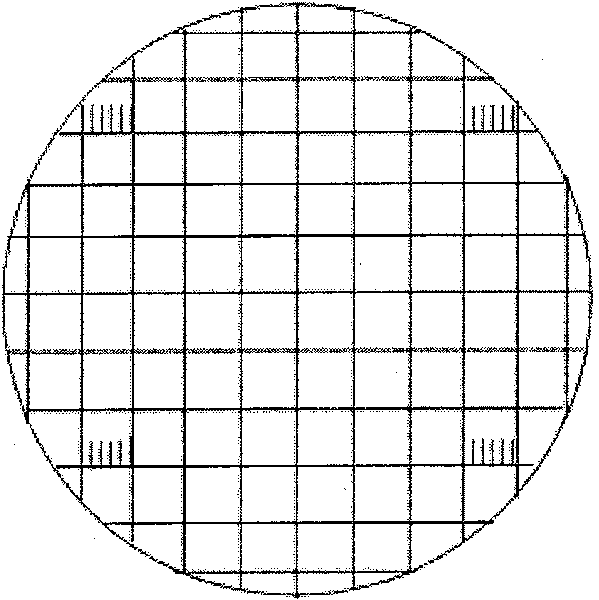
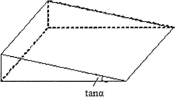
[0056] Taking the printed board (sample 1) that has undergone the electroplating nickel / gold plating process, the thickness of the Ni layer is measured to be 3.324 μm, and the thickness of the Au layer is 0.125 μm. Put the sample in the above-mentioned test solution at a temperature of 22°C for 5 minutes after the oil is removed, blot it dry with absorbent paper, and observe it under a 20X optical microscope. When observing, use a transparent square mesh with a line width of 0.1 mm and a spacing of 1 mm. The Gefferin negative film is installed under the eyepiece of the low power microscope. The inclined plane with an inclination angle of tanα between 0.15 and 0.25 is a inclined plane made of rubber or...

Embodiment 2

[0058] According to the method of Example 1, prepare 250 ml of test solution with hydrochloric acid concentration of 2.3%, sodium chloride concentration of 1.0%, and penetrant concentration of 0.05%.

[0059] Taking the printed board (sample 2) after electroplating nickel / thick gold plating process, the thickness of the Ni layer was measured to be 6.570 μm, and the thickness of the Au layer was 0.520 μm. Put sample 2 into the above-mentioned test solution at 21°C for 8 minutes after removing the oil, blot it dry with absorbent paper, and observe it under a 20X optical microscope. When observing, use a transparent square mesh with a line width of 0.1 mm and a spacing of 1 mm. The Gefferin film is installed under the eyepiece of the low-power microscope. The inclined plane with an inclination angle of tanα between 0.15 and 0.25 is a inclined plane made of rubber or wood with the same inclination angle of tanα. The final porosity calculated according to Table-1 is 0.3 / cm 2 .

Embodiment 3

[0061] According to the method of Example 1, 250 ml of test solutions with hydrochloric acid concentration of 2.5%, sodium chloride concentration of 1.5%, and penetrant concentration of 0.1% were prepared.

[0062] Taking the printed board (sample 3) subjected to the immersion soft nickel / immersion gold process, the thickness of the Ni layer was measured to be 1.248 μm, and the thickness of the Au layer was 0.070 μm. Put the sample 3 into the above-mentioned test solution at a temperature of 22°C for 5 minutes after removing the oil stains, blot it dry with absorbent paper, and observe it under a 20X optical microscope. When observing, use a transparent square mesh with a line width of 0.1 mm and a spacing of 1 mm. The Gefferin film is installed under the eyepiece of the low-power microscope. The inclined plane with the inclination angle tanα between 0.15 and 0.25 is a inclined plane with the same inclination angle tanα made of rubber or wood. The final porosity calculated acco...


PUM

PropertyMeasurementUnit
thicknessaaaaaaaaaa
thicknessaaaaaaaaaa
thicknessaaaaaaaaaa

Abstract

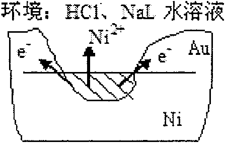
The invention provides an inspection method of printed circuit board gold plating layer porosity, which belongs to the field of the chemical industry technique, relating to the detection of the printed circuit board surface gold plating layer, and particularly is suitable for detecting the printed plate conducting wire and the porosity of golden finger gold plating layer. The principal ingredientof the test solution is HCl, NaCl and osmotic agent, which produces obvious corrosion products at the discontinuous points of the gold plating layer at a certain temperature and time, transparent gridmaterial with graduates and clinohedral are used for supplementary observation, pore space sizes are weighted processed, the porosity is observed and calculated under the microscope. The invention has the merits of fast speed, convenience, accuracy and safety, which meets the surface quality detection need in the production process of the printed circuit board.

Description

technical field [0001] The invention belongs to the technical field of chemical industry, relates to the detection of the gold-plated layer on the surface of a printed circuit board, and is especially suitable for the detection of the porosity of the gold-plated layer of the lead wire of the printed circuit board and the gold finger. Background technique [0002] The rise of surface mount technology (SMT) requires the metal coating on the surface of the printed circuit board pad to have the characteristics of anti-oxidation, high solderability, high conductivity and high heat dissipation. Organic Solderability Preservatives OSP, electroless nickel-gold or electroplated nickel-gold surface treatment can well meet the requirements of SMT soldering and are widely used in industrial production. [0003] The disadvantage of the organic solderability protective coating (OSP) process is that the formed protective film is extremely thin and easy to be scratched (or scratched), so it...

Claims


Application Information

Patent Timeline
Patent Type & Authority Patents(China)
IPC IPC(8): G01N15/08
Inventor 何为赵丽王守绪何波汪洋林均秀徐玉珊
Owner UNIV OF ELECTRONICS SCI & TECH OF CHINA
Learn More