

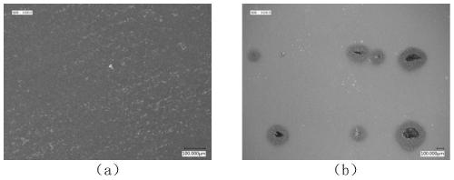
Method for detecting residual copper layer distribution of printed circuit board
A technology for printed circuit boards and copper layers, which is applied in the direction of chemical reaction of materials and material analysis by observing the influence of chemical indicators, so as to achieve the effect of simple detection method and meet the requirements of surface quality detection.
- Summary
- Abstract
- Description
- Claims
- Application Information
AI Technical Summary
Problems solved by technology
Method used
Image

Examples
Embodiment 1
[0030] (1) Preparation of auxiliary solution and detection solution
[0031] Preparation of auxiliary solution: Add 200ml of deionized water into a 500mL beaker, pipette 20ml of concentrated hydrochloric acid into the beaker, and stir. Weigh 5g of stannous chloride, add a small amount to the beaker several times, and stir. Finally add deionized water to the 500mL mark;
[0032] Preparation of test solution: Add 200ml of deionized water into a 500mL beaker, pipette 5ml of concentrated hydrochloric acid into the beaker, and stir. Weigh 0.125g of palladium chloride, add deionized water into the beaker, and stir. Finally add deionized water to the 500mL mark.
[0033] (2) Making printed circuit boards
[0034] The substrate goes through the pre-processing line and enters the exposure process. The model DG-38 photoresist dry film is pasted on the substrate, the circuit data is uploaded and the exposure energy of the LDI exposure machine is set to 16KJ for exposure. When expose...
Embodiment 2
[0039] (1) Preparation of auxiliary solution and detection solution
[0040]Preparation of auxiliary solution: Add 200ml of deionized water into a 500mL beaker, pipette 5ml of concentrated hydrochloric acid into the beaker, and stir. Weigh 20g of stannous chloride, add a small amount to the beaker several times, and stir. Finally add deionized water to the 500mL mark;
[0041] Preparation of test solution: Add 200ml of deionized water into a 500mL beaker, pipette 5ml of concentrated hydrochloric acid into the beaker, and stir. Weigh 0.25g of palladium chloride, add deionized water into the beaker, and stir. Finally add deionized water to the 500mL mark.
[0042] (2) Making printed circuit board circuits
[0043] The substrate goes through the pre-processing line and enters the exposure process. The model DG-38 photoresist dry film is pasted on the substrate, the circuit data is uploaded and the exposure energy of the LDI exposure machine is set to 16KJ for exposure. When ...
Embodiment 3
[0047] (1) Preparation of auxiliary solution and detection solution
[0048] Auxiliary solution preparation: Add 200ml of deionized water into a 500mL beaker, pipette 55ml of concentrated hydrochloric acid into the beaker, and stir. Weigh 50g of stannous chloride, add a small amount to the beaker several times, and stir. Finally add deionized water to the 500mL mark;
[0049] Preparation of test solution: Add 200ml of deionized water into a 500mL beaker, pipette 5ml of concentrated hydrochloric acid into the beaker, and stir. Weigh 0.1 g of palladium chloride, add deionized water into the beaker, and stir. Finally add deionized water to the 500mL mark.
[0050] (2) Making printed circuit board circuits
[0051] The substrate goes through the pre-processing line and enters the exposure process. The dry film of Hitachi 1333 photoresist is used to paste the substrate on the substrate. The circuit data is uploaded and the exposure energy of the LDI exposure machine is set to 1...
PUM
 Abstract
Description
Claims
Application Information