

Film forming composition for nanoimprinting and method for pattern formation
A technology of nano-imprinting and composition, applied in the directions of nanotechnology, nanotechnology, nanotechnology for information processing, etc., can solve problems such as yield decline, transfer pattern peeling, photoresist heating, etc., and achieve the effect of high yield
Active Publication Date: 2008-09-03
TOKYO OHKA KOGYO CO LTD
View PDF2 Cites 20 Cited by
- Summary
- Abstract
- Description
- Claims
- Application Information
AI Technical Summary
Problems solved by technology
[0007] However, thermal cycle nanoimprint lithography has the following problems: decrease in yield due to time taken for temperature rise and cooling of the photoresist, dimensional change due to temperature difference, decrease in accuracy of transfer patterns, and thermal expansion. The alignment accuracy drops, etc.
Therefore, the transfer pattern formed on the substrate will be peeled off, so further improvement is required.
Method used
View moreImage
Smart ImageViewing Examples

Examples
Embodiment 1
[0176] 1 mol of tetraethoxysilane, 0.5 mol of monoacryloxypropyltrimethoxysilane and 0.5 mol of monovinyltrimethoxysilane were dissolved in 170 g of isopropanol. Next, 190 g of pure water and 0.02 g of concentrated nitric acid were added, followed by stirring at room temperature for 6 hours. The resulting composition was then diluted with isopropanol so that the SiO 2 The converted solid content value was 7%. Next, 1 g of photopolymerization initiator IRGACURE 369 (manufactured by Ciba Specialty Chemicals: 2-benzyl-2-dimethylamino-1-(4-morpholinophenyl) butan-1-one) was added to 100 g of the obtained liquid, to prepare coating solutions.
Login to View More PUM
 Abstract
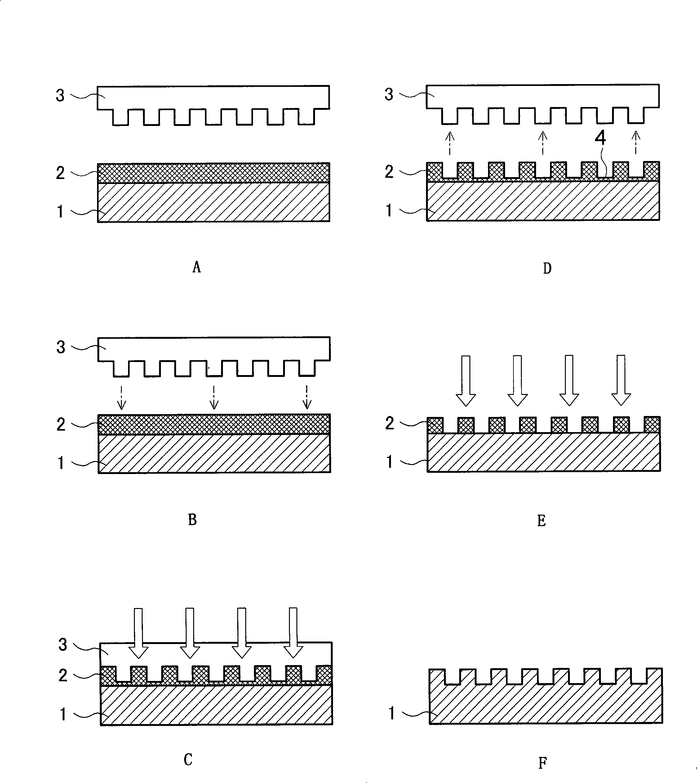
This invention provides a film forming composition for nanoimprinting, which has excellent resistance to etching with oxygen gas, can prevent the separation of a transfer pattern, can eliminate a problem of a holing time on a substrate, and is also excellent in transferability, and photosensitive resist, a nanostructure, a method for pattern formation using the same, and a program for realizing the method for pattern formation. The film forming composition for nanoimprinting comprises a polymeric silicon compound having the function of causing a photocuring reaction. Preferably, the polymericsilicon compound has a functional group cleavable as a result of response to electromagnetic waves and causes a curing reaction upon exposure to electromagnetic waves. More preferred are siloxane polymer compounds, silicon carbide polymer compounds, polysilane polymer compounds, and silazane polymer compounds, or any mixture thereof.
Description
technical field [0001] The present invention relates to a film-forming composition for nanoimprinting and a pattern-forming method using the composition. More specifically, the present invention relates to a film-forming composition for nanoimprint, a photosensitive photoresist, a nanostructure, a pattern forming method using them, and a method for realizing the photocuring reaction. The program of the pattern forming method described above. Background technique [0002] Photolithography technology is the core technology of semiconductor device technology. With the high integration of semiconductor integrated circuits (IC) in recent years, wiring has further developed towards miniaturization. In particular, in a semiconductor integrated circuit called a super large scale integrated circuit (Super Large Scale Integrated Circuit, super LSI) whose integration degree exceeds 10 million elements, microfabrication lithography technology must be used. [0003] The microfabricatio...
Claims
Login to View More Application Information
Patent Timeline
 Patent Type & AuthorityApplications(China)
IPC IPC(8): B29C59/02H01L21/027G03F7/075C09D183/00
CPCG03F7/0757B82Y10/00H01L21/0273G03F7/0002C09D183/04C08G77/20B82Y40/00Y10T156/1041Y10T428/24802G03F7/035B29C59/02B82B1/00B82B3/00
Inventor坂本好谦山下直纪石川清
OwnerTOKYO OHKA KOGYO CO LTD