Liquid crystal device, method of manufacturing liquid crystal device, and electronic apparatus

A technology of liquid crystal device and manufacturing method, applied in semiconductor/solid-state device manufacturing, circuits, transistors, etc., can solve problems such as poor friction, poor orientation, and increased resistance, and achieve the effect of reducing poor alignment and optimizing film thickness balance

Active Publication Date: 2008-10-01
JAPAN DISPLAY INC
View PDF1 Cites 10 Cited by
  • Summary
  • Abstract
  • Description
  • Claims
  • Application Information

AI Technical Summary

Problems solved by technology

[0007] However, if shown in Figure 7 (a), Figure 7 If the rubbing process is performed in the configuration of (b), there is a problem that there is a large step in the thickness of the common electrode 9a on the side of the common electrode 9a in the direction of travel of the rubbing roller relative to the common electrode 9a inside the gap portion 9b of the common electrode 9a. The difference leads to the generation of friction defect 16a in a wide range, and such friction defect 16a becomes a cause of a decrease in the quality of a displayed image such as a decrease in contrast.
However, if the film thickness of the common electrode 9a and the pixel electrode 7a is thinned, the resistance of the common electrode 9a increases, and this increase in resistance becomes a cause of occurrence of luminance unevenness in an image, etc.
[0008] In addition to the aforementioned rubbing defect, if the thickness of the common electrode 9a is thick, poor alignment may also occur due to the level difference itself, or may be caused by the gap between the region where the common electrode 9a is formed in the pixel and the slit-shaped gap portion 9b. Changes in the thickness of the liquid crystal layer may also reduce the contrast of the display

Method used


Image

  • Liquid crystal device, method of manufacturing liquid crystal device, and electronic apparatus
  • Liquid crystal device, method of manufacturing liquid crystal device, and electronic apparatus
  • Liquid crystal device, method of manufacturing liquid crystal device, and electronic apparatus

Examples


Embodiment approach 1

[0033] (overall composition)

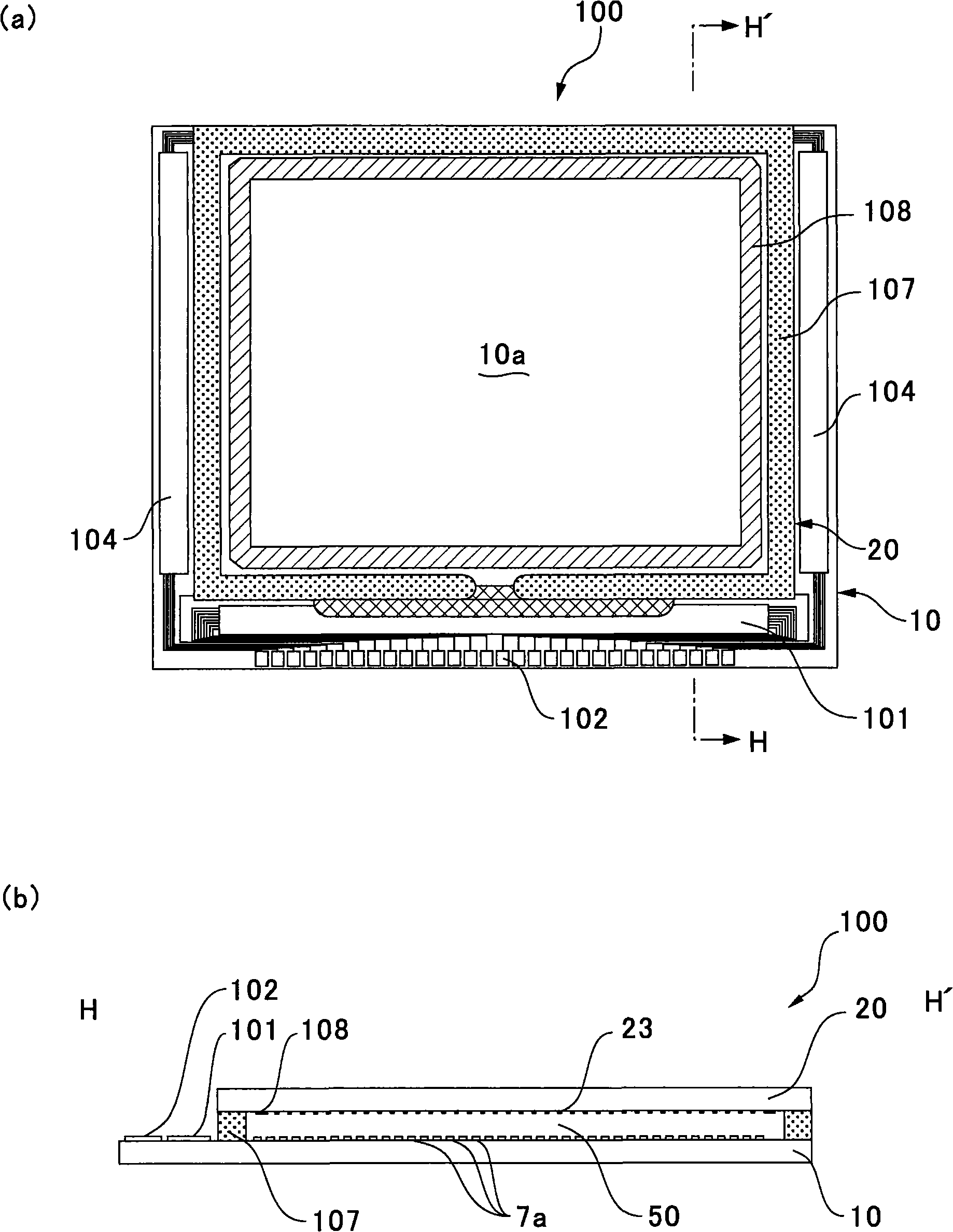
[0034] figure 1 (a) and (b) are a plan view and a H-H' sectional view of a liquid crystal device to which the present invention is applied and components formed thereon viewed from the counter substrate side, respectively.

[0035] exist figure 1 (a), figure 1 In (b), the liquid crystal device 100 of this embodiment is a transmissive active matrix liquid crystal device, and the sealing material 107 is provided along the edge of the counter substrate 20 on the element substrate 10 . In the element substrate 10, in the area outside the sealing material 107, the data line driving circuit 101 and the mounting terminal 102 are arranged along one side of the element substrate 10, and the scanning line driving circuit is formed along the two sides adjacent to the side where the mounting terminal 102 is arranged. circuit 104. Furthermore, peripheral circuits such as a precharge circuit and an inspection circuit may be provided under the frame 108 ...

Embodiment approach 2

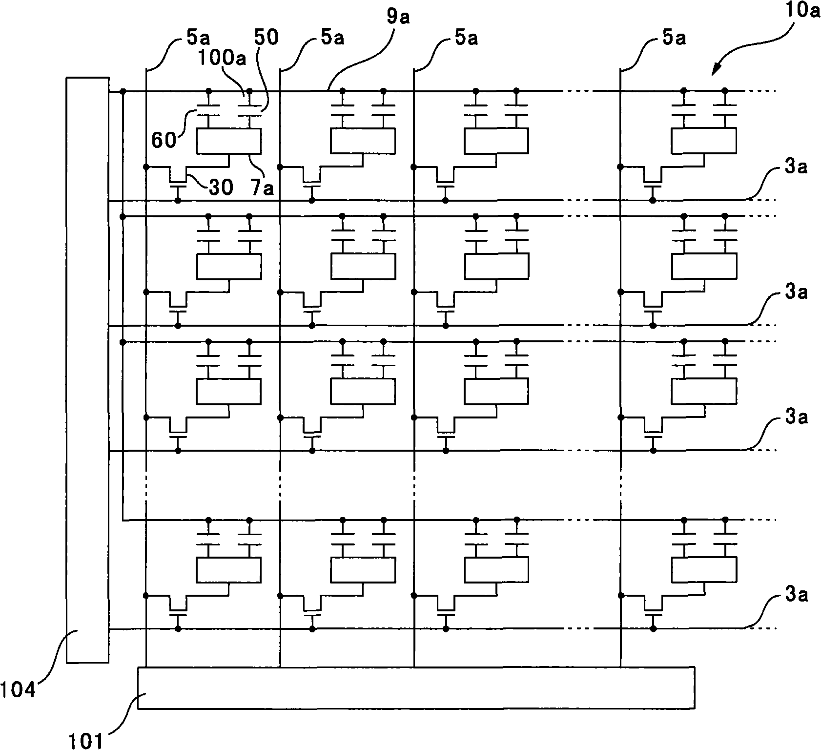
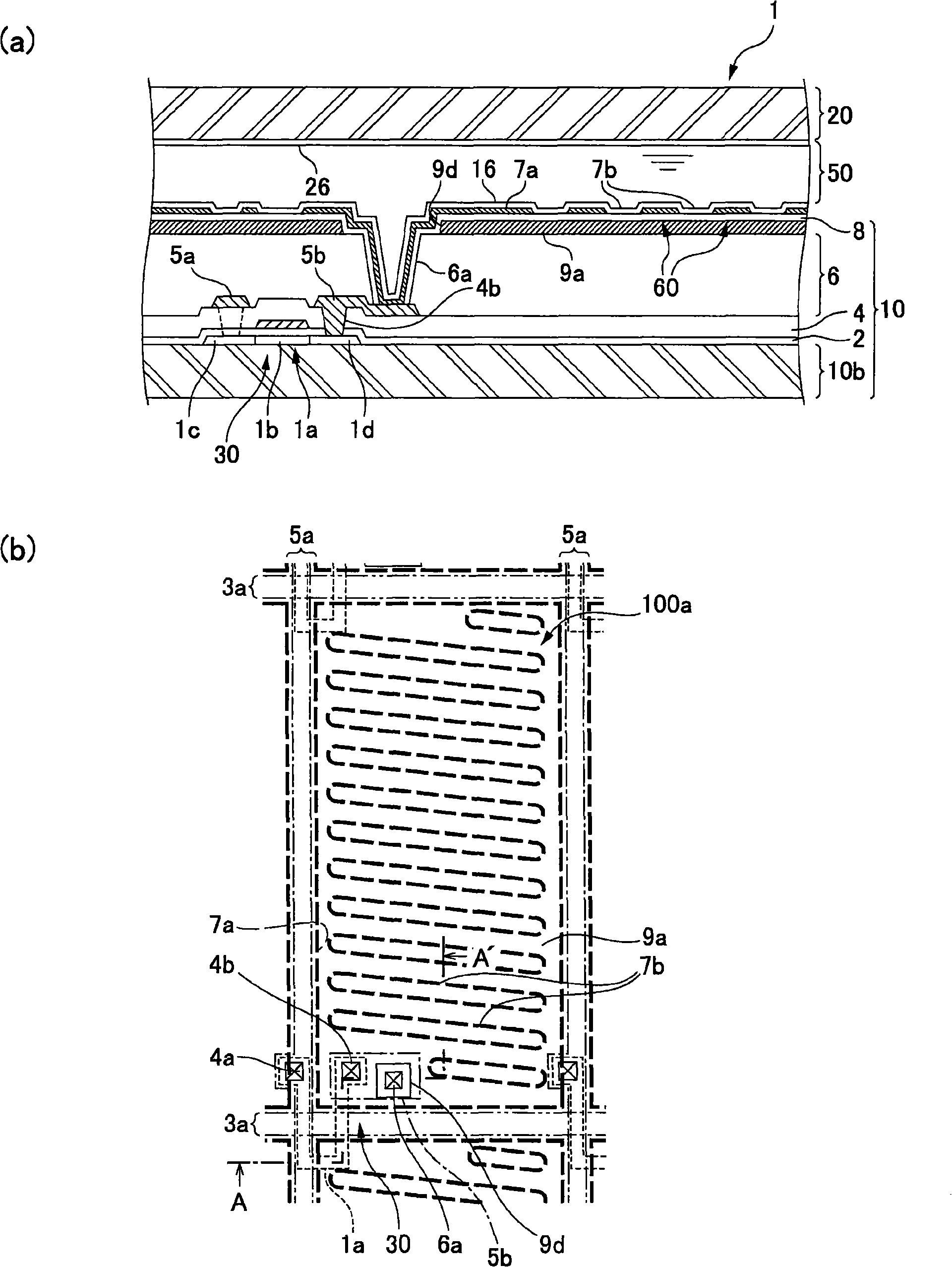
[0061] Figure 5 (a) and (b) are respectively a sectional view corresponding to one pixel of the liquid crystal device 100 in Embodiment 2 of the present invention and a plan view of pixels adjacent to the element substrate 10; Figure 5 (a), which is equivalent to image 3 The position of line B-B' in (b) is a cross-sectional view when the liquid crystal device 100 is cut. In addition, since the basic structure of this embodiment is the same as that of Embodiment 1, the same code|symbol is attached|subjected to the same part, and their description is abbreviate|omitted.

[0062] as shown in Figure 5 (b), on the element substrate 10, a plurality of transparent pixel electrodes 7a (regions surrounded by long dotted lines) are formed in a matrix for each pixel 100a, and data are formed along the vertical and horizontal boundary regions of the pixel electrodes 7a. Line 5a (indicated by a one-dot chain line), and scanning line 3a (indicated by a two-dot chain line). In additi...


PUM

PropertyMeasurementUnit
thicknessaaaaaaaaaa
thicknessaaaaaaaaaa
thicknessaaaaaaaaaa

Abstract

The invention relates to a liquid crystal device, a manufacturing method of the liquid crystal device, and an electric device. The invention provides a liquid crystal device capable of inhibiting FFS mode of occurrence of friction disorder without increasing resistance of an electrode layer. On an element substrate (10) of the liquid crystal device (100), an upper layer side of a film transistor (30) is covered by an interlayer insulated film (6) made from an organic flattened film; on the upper layer of the interlayer insulated film (6), a common electrode (9a) is formed as an electrode layer of the whole surface. An inter-electrode insulated film (8) forms on the upper layer of the shared electrode (9a). A pixel electrode (7a) with a gap part (7b) with seam shaped forms on the inter-electrode insulated film (8). Compared to the common electrode (9a) on the whole surface, the pixel electrode (7a) with the gap part (7b) of seam shape has thin film thickness, so that the pixel electrode (7a) is capable of undergoing friction treatment appropriately.

Description

technical field [0001] The present invention relates to a liquid crystal device, and particularly relates to an element substrate including both a pixel electrode and a common electrode, which is represented by a so-called fringe field switching (hereinafter referred to as FFS (Fringe Field Switching)) mode liquid crystal device. Technology of liquid crystal devices. Furthermore, it relates to a method of manufacturing the liquid crystal device and electronic equipment to which the liquid crystal device is applied. Background technique [0002] In the FFS mode liquid crystal device among various liquid crystal devices, pixel electrodes, inter-electrode insulating films, and common electrodes with gaps are formed on the element substrate among the element substrate and the counter substrate. The liquid crystal is driven by an electric field with the common electrode (see Patent Document 1). [0003] [Patent Document 1] JP-A-2001-235763 [0004] In such an FFS mode liquid c...

Claims


Application Information

Patent Timeline
Patent Type & Authority Applications(China)
IPC IPC(8): G02F1/1343G02F1/1362H01L21/84
CPCG02F2201/12G02F1/133357G02F1/134372H01L29/786
Inventor 藤田伸
Owner JAPAN DISPLAY INC
Why Eureka
Try Eureka