A kind of preparation method of near-single crystal double-layer transparent aln ceramic composite substrate

A technology of transparent ceramics and ceramic composites, applied in the direction of single crystal growth, single crystal growth, chemical instruments and methods, etc., can solve the problem that the single crystal structure cannot be grown, the growth of AlN single crystal or GaN single crystal is hindered, and the AlN transparent cannot be formed. Ceramic structure, etc.

Active Publication Date: 2021-10-15
SINO INNOV SEMICON (PKU) CO LTD
View PDF3 Cites 0 Cited by
  • Summary
  • Abstract
  • Description
  • Claims
  • Application Information

AI Technical Summary

Problems solved by technology

However, due to the lack of GaN single crystal substrates, the substrate material currently used in GaN-based LED devices is still Al 2 o 3 (sapphire) substrate as the main substrate material
After the development of sapphire substrate in recent years, great progress has been made, but there are still key problems that cannot be overcome. First, the sapphire substrate and its epitaxial GaN or AlN material are still heterogeneous epitaxial substrates. The lattice mismatch with GaN reaches 13.6%, and the thermal mismatch exceeds 50%. The result of this problem is that after growing GaN on the sapphire substrate, the epitaxial wafer generally warps seriously, and the 4-inch sapphire / GaN epitaxial wafer warps The curvature reaches more than 200 microns. At the same time, in order to overcome the warpage, the 4-inch sapphire substrate is more than twice as thick as the 2-inch sapphire substrate, just to balance the lattice mismatch and thermal mismatch of GaN Warpage caused by stress. On this basis, GaN devices grown on sapphire substrate materials cannot be developed to 6 inches and 8 inches, because the thickness of sapphire has to be increased more, and the warpage problem faced at the same time is almost impossible. overcome
At the same time, such problems are more serious when growing AlN on sapphire substrates
Second, the thermal conductivity of the sapphire substrate is very poor, about 25W / mk, and the development of GaN and AlN-based devices is increasingly moving towards power and miniaturization, and the device power is getting higher and higher, and the heat generation The sapphire substrate is getting bigger and bigger, and the sapphire substrate is becoming more and more the heat dissipation bottleneck of the device. Its poor heat dissipation will cause the junction temperature of the device to rise rapidly, which will cause problems such as device failure and a significant decrease in life.
Therefore, from this point of view, it is very suitable to use AlN ceramic substrates as substrate materials for GaN-based and AlN-based devices. However, the existing AlN ceramic substrates have a single-layer structure with only one layer of ceramics. Ceramic properties, polycrystalline materials, the grain size is about 3-5 microns, the crystal orientation is disordered, and the c-axis crystal orientation is disordered; and the existing preparation of AlN ceramic substrates mainly uses tape casting technology, which requires the use of colloid, diffusion Additives and sintering aids: such as yttrium oxide, etc., its impurity quantity and content are high, and it is impossible to form AlN transparent ceramic structure
Under the guidance of the material growth theory, it is impossible to grow a single crystal structure on a polycrystalline structure, and impurities such as sintering aids have a great hindering effect on the growth of AlN single crystal or GaN single crystal on the AlN ceramic substrate. It is theoretically impossible to grow GaN single crystal on some AlN ceramic substrates

Method used


Image

  • A kind of preparation method of near-single crystal double-layer transparent aln ceramic composite substrate

Examples


Embodiment 1

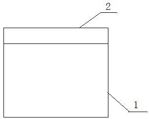
[0028] Embodiment 1, a preparation method of a near-single-crystal double-layer transparent AlN ceramic composite substrate, which includes the following steps, the near-single-crystal double-layer transparent AlN ceramic composite substrate includes a lower near-single-crystal AlN transparent ceramic substrate and an upper layer AlN or GaN quasi-single-crystal layer; the thickness of the near-single-crystal AlN transparent ceramic substrate is 100 microns, the unit cell diameter is 1 micron, does not contain sintering aids, and the c-axis orientation deviation is within 10-20°; the AlN Or the thickness of the GaN quasi-single crystal layer is 5 microns, and the c-axis orientation deviation is within 5°.

[0029] A. The preparation of the near-single-crystal AlN transparent ceramic substrate with the c-axis deviation within 10-20°, which includes the following steps: (1) preparing a powder whose particle size is within 1 micron and the impurity content is less than 0.1%. Pure ...

Embodiment 2

[0033] Embodiment 2, a preparation method of a near-single-crystal double-layer transparent AlN ceramic composite substrate, which includes the following steps, the near-single-crystal double-layer transparent AlN ceramic composite substrate includes a lower near-single-crystal AlN transparent ceramic substrate and an upper layer AlN or GaN quasi-single crystal layer; the thickness of the near-single crystal AlN transparent ceramic substrate is 500 microns, the unit cell diameter is 3 microns, does not contain sintering aids, and the c-axis orientation deviation is within 10-20°; the AlN Or the thickness of the GaN quasi-single crystal layer is 50 microns, and the c-axis orientation deviation is within 5°.

[0034] A. The preparation of the near-single-crystal AlN transparent ceramic substrate with the c-axis deviation within 10-20°, which includes the following steps: (1) preparing a powder whose particle size is within 1 micron and the impurity content is less than 0.1%. Pur...

Embodiment 3

[0038] Embodiment 3, a preparation method of a near-single-crystal double-layer transparent AlN ceramic composite substrate, which includes the following steps, the near-single-crystal double-layer transparent AlN ceramic composite substrate includes a lower near-single-crystal AlN transparent ceramic substrate and an upper layer AlN or GaN quasi-single crystal layer; the thickness of the near-single crystal AlN transparent ceramic substrate is 1000 microns, the unit cell diameter is 1.5 microns, does not contain sintering aids, and the c-axis orientation deviation is within 10-20°; the AlN Or the thickness of the GaN quasi-single crystal layer is 10 microns, and the c-axis orientation deviation is within 5°.

[0039] A. The preparation of the near-single-crystal AlN transparent ceramic substrate with the c-axis deviation within 10-20°, which includes the following steps: (1) preparing a powder whose particle size is within 1 micron and the impurity content is less than 0.1%. ...


PUM

PropertyMeasurementUnit
particle diameteraaaaaaaaaa
thicknessaaaaaaaaaa
thicknessaaaaaaaaaa

Abstract

The invention discloses a method for preparing a near-single-crystal double-layer transparent AlN ceramic composite substrate. The near-single crystal has a c-axis deviation within 10-20°, a thickness of 100-1000 microns, and a unit cell diameter of 1-3 microns. Preparation of AlN transparent ceramic substrate: Put the pure AlN ceramic powder into a plastic bag to form a cylindrical shape, put it into a warm isostatic pressing equipment for pressing and crushing, and press it twice, cut it into substrate discs and put them in a sintering furnace for two times. Sub-high temperature sintering; preparation of AlN or GaN quasi-single crystal layers with a c-axis orientation deviation within 5° and a thickness of 5-100 microns on a transparent ceramic substrate: prepared by methods such as molecular beam epitaxy or metal organic compound vapor deposition, high temperature sintering. The composite substrate prepared by the invention can realize epitaxial growth of GaN or AlN single crystal material or device, has small warping deformation, high thermal conductivity, low manufacturing cost, and makes it possible to produce 6-inch and 8-inch LED devices.

Description

technical field [0001] The invention belongs to the field of semiconductor material preparation, and relates to a method for preparing a nearly single-crystal double-layer transparent AlN ceramic composite substrate. Background technique [0002] With the development and application of GaN or AlN-based device technology, the general lighting and light emitting fields in the world are basically monopolized by GaN or AlN-based devices. However, due to the lack of GaN single crystal substrates, the substrate material currently used in GaN-based LED devices is still Al 2 o 3 (sapphire) substrate as the main substrate material. After the development of sapphire substrate in recent years, great progress has been made, but there are still key problems that cannot be overcome. First, the sapphire substrate and its epitaxial GaN or AlN material are still heterogeneous epitaxial substrates. The lattice mismatch with GaN reaches 13.6%, and the thermal mismatch exceeds 50%. The resul...

Claims


Application Information

Patent Timeline
Patent Type & Authority Patents(China)
IPC IPC(8): H01L21/02H01L33/00C30B23/02C30B25/18C30B29/40
Inventor 孙永健郭坚王光普谌洛贾军峰豆学刚莫少琼
Owner SINO INNOV SEMICON (PKU) CO LTD
Why Eureka
Try Eureka