

Method for preparing thin type press key panel
A manufacturing method and thinning technology, applied in electrical components, electrical switches, circuits, etc., can solve problems such as increased steps or procedures, increased man-hours, increased button thickness, etc.
- Summary
- Abstract
- Description
- Claims
- Application Information
AI Technical Summary
Problems solved by technology
Method used
Image

Examples
Embodiment Construction
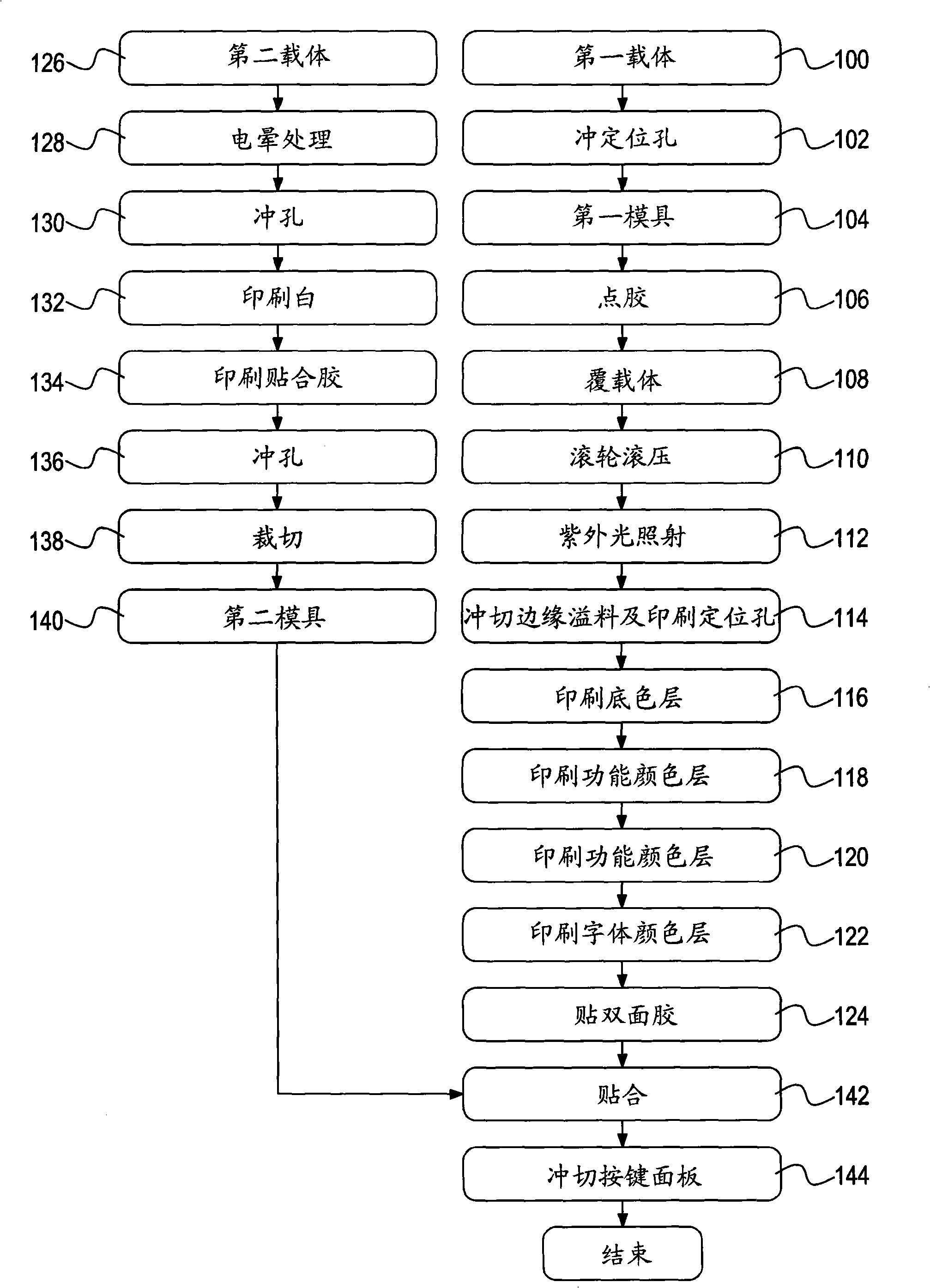
[0037] The technical content of the present invention will be described in detail below in conjunction with the accompanying drawings:
[0038] See Figure 2A , Is a schematic diagram of the manufacturing process of the first thin button of the present invention. The figure discloses a method for manufacturing a button structure with a pattern layer button. First, as in step 100, a carrier 2 made of a transparent material of a polycarbonate film (PC Film) is prepared.
[0039] Step 102, please refer to image 3 , Punch a positioning hole 21 on the surface of the first carrier 2, and the positioning hole 21 is used to provide the first carrier 2 to be positioned on the positioning post 13 of the first mold 1.
[0040] Step 104, please refer to Figure 4 , Equipped with a first mold 1, in the first mold 1 has a first mold cavity 11, the first mold cavity 11 has a plurality of second mold cavities 12, the second mold cavity 12 is used to shape the shape of the button, and The bottom ...
PUM
 Abstract
Description
Claims
Application Information