
Joining method, display apparatus and display

A bonding method and display device technology, which can be applied to static indicators, instruments, nonlinear optics, etc., and can solve the problems of large size of liquid crystal display devices, etc.

Inactive Publication Date: 2008-10-15
INNOLUX CORP
View PDF0 Cites 4 Cited by
  • Summary
  • Abstract
  • Description
  • Claims
  • Application Information

AI Technical Summary

Problems solved by technology

However, a larger space must be reserved on the gate side and the source side of the display device 50″ for the connection of the flexible circuit boards 36, 38.
Therefore, the size of the liquid crystal display device 50" produced by the double-sided grain-glass bonding method is relatively large.

Method used


Image

  • Joining method, display apparatus and display
  • Joining method, display apparatus and display
  • Joining method, display apparatus and display

Examples


Embodiment Construction

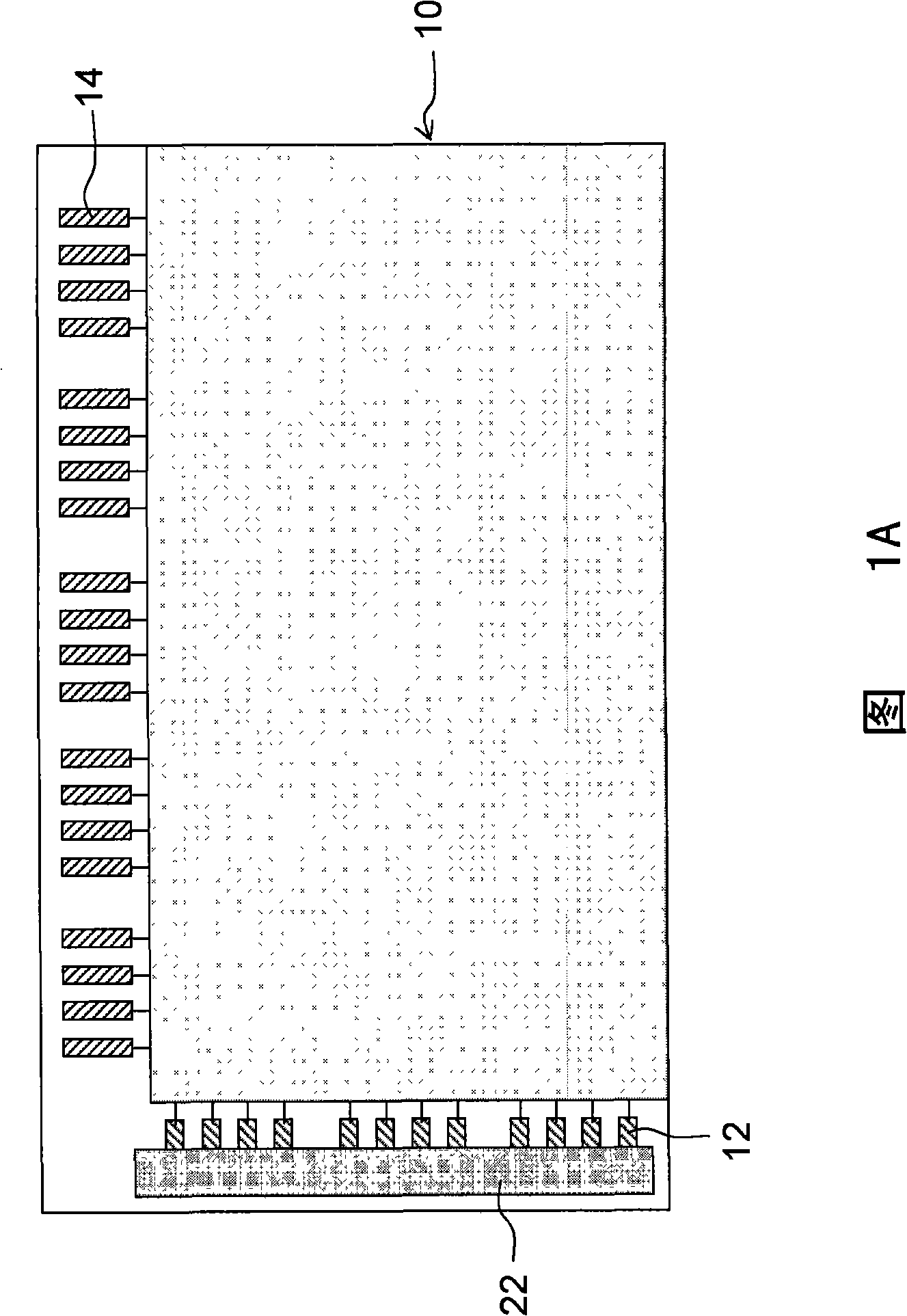
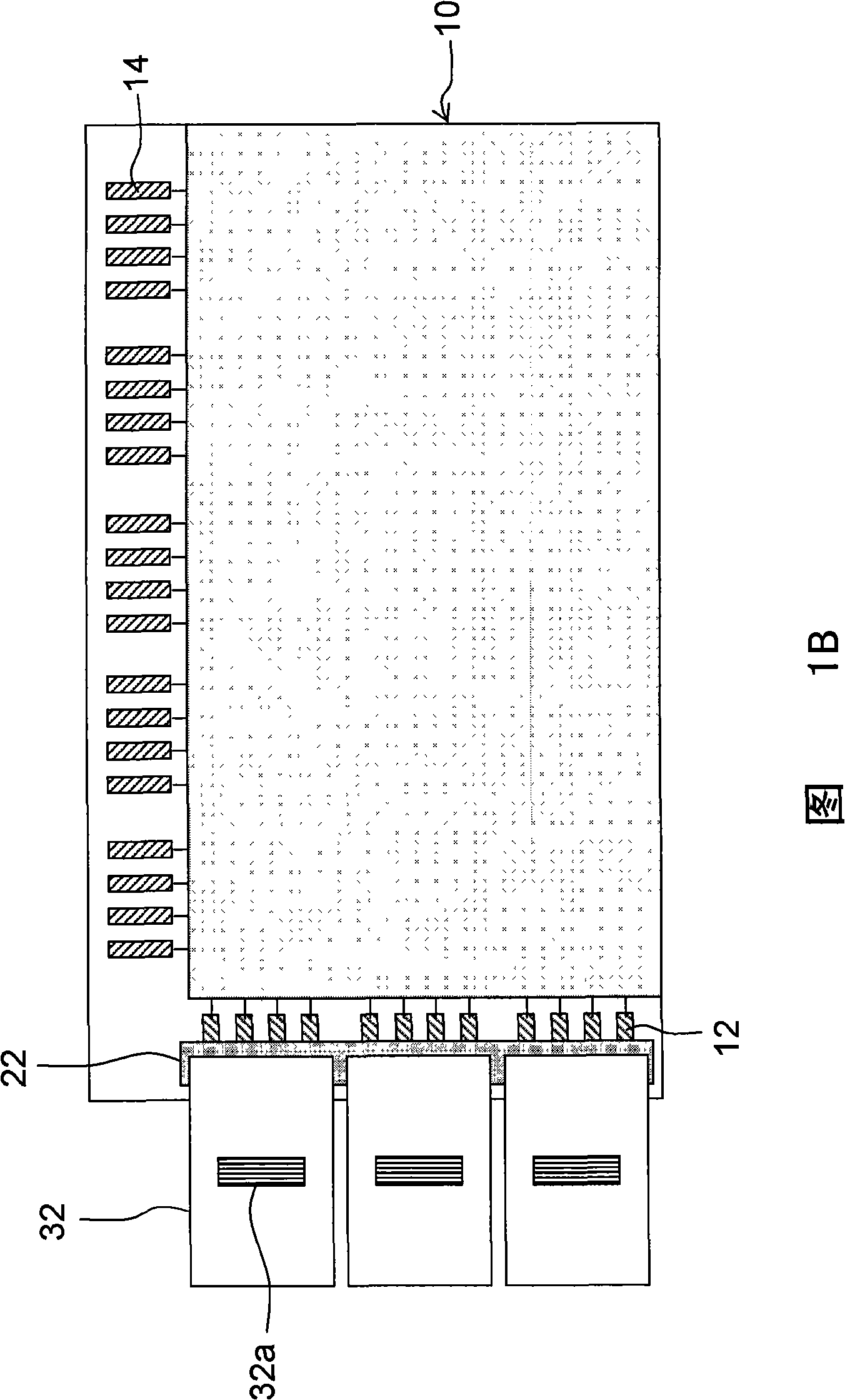
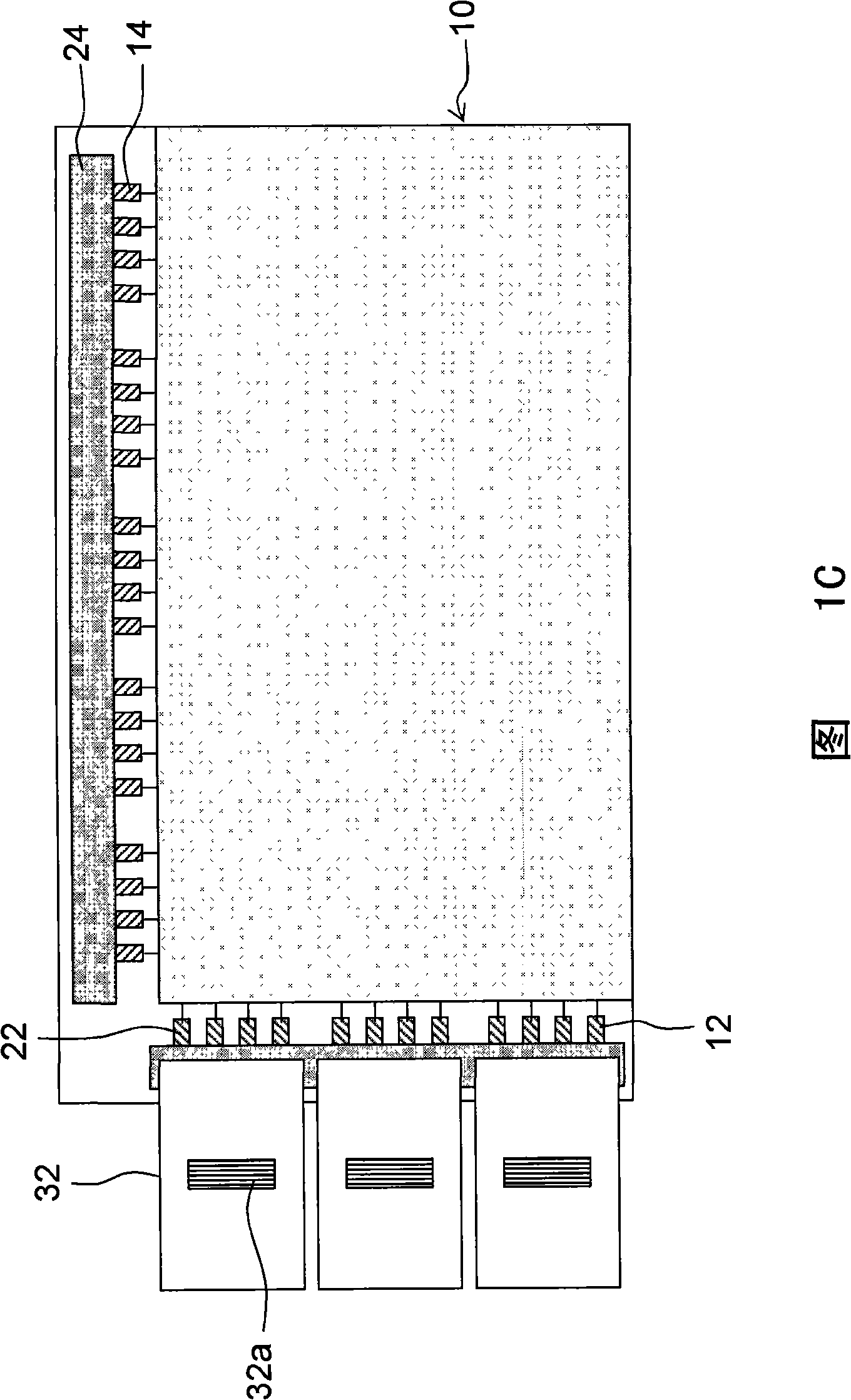
[0078] FIG. 5 is a top view of a display device according to an embodiment of the present invention. Referring to FIG. 5 , the display device 100 includes a display panel 110 , a plurality of first chips 120 , a plurality of second chips 130 , at least one flexible circuit board 140 and a printed circuit board 150 . The display panel 110 has a display area 112 , a first peripheral circuit area 114 and a second peripheral circuit area 116 . Both the first peripheral circuit area 114 and the second peripheral circuit area 116 are adjacent to the display area 112 . However, in another embodiment, the first peripheral circuit area 114 and the second peripheral circuit area 116 may not be adjacent to the display area 112 . In addition, a plurality of first pads 114 a are disposed in the first peripheral circuit area 114 , and a plurality of second pads 116 a are disposed in the second peripheral circuit area 116 . The first chip 120 is disposed on the first peripheral circuit are...


PUM


Abstract

The invention discloses a joint method suitable for jointing a display panel and a plurality of chips. A plurality of first join pads are arranged in a first peripheral circuit territory of the display panel, and a plurality of second joint pads are arranged in a second periphery circuit territory of the display panel. The joint method comprises the following steps: first, a first anisotropic conductive adhesive is attached to the first joint pad; a plurality of first chips are arranged on the first anisotropic adhesive; the first pressing manufacture process is carried out so that the first chips are electrically connected with the first joint pads; a second anisotropic conductive adhesive is attached to the second joint pads; and a plurality of second chips and at least one flexible circuit board are arranged on the second anisotropic conductive adhesive; then the second pressing manufacture process is carried out, so that the second chips and one end of the flexible circuit board are electrically connected with the second joint pads through the second anisotropic conductive adhesive. The joint method provided by the invention makes use of few steps to joint the plurality of chips and the display panel, thereby reducing manufacturing cost of a display device.

Description

technical field [0001] The present invention relates to a bonding method (bonding method), a display apparatus (display apparatus) and a display (display device), and in particular to a bonding method for manufacturing a display apparatus, a display apparatus with low manufacturing cost and Make displays that cost less to make. Background technique [0002] In order to match the modern life style, the volume of video or image devices is becoming thinner and lighter. Although the traditional cathode ray tube (CRT) display still has its advantages, due to the structure of its internal electronic cavity, the CRT display is bulky and takes up a lot of space. At the same time, radiation will be generated, causing eye damage and other problems. Therefore, flat panel displays (FPDs), such as liquid crystal display apparatuses, developed in conjunction with optoelectronic technology and semiconductor manufacturing technology, have gradually become the mainstream of display product...

Claims


Application Information

Patent Timeline
IPC IPC(8): G02F1/1345G02F1/133
Inventor 黄国钦
Owner INNOLUX CORP
Learn More