Panel/wafer molding apparatus and method of the same

A technology of packaging equipment and packaging methods, which is applied in semiconductor/solid-state device manufacturing, electrical components, and electrical solid-state devices, etc., can solve the problems of expensive packaging process, prone to warpage, and easy damage.

Inactive Publication Date: 2008-10-29
ADVANCED CHIP ENG TECH INC
View PDF0 Cites 4 Cited by
  • Summary
  • Abstract
  • Description
  • Claims
  • Application Information

AI Technical Summary

Problems solved by technology

The traditional flat / wafer structure packaging process is expensive and has other disadvantages, including: the assembly of these tools takes a long time, the wafer or flat structure is easily damaged during the molding process, and warpage is prone to occur during the process, and the need to use special tape or Tools to protect wafer and flat structures

Method used


Image

  • Panel/wafer molding apparatus and method of the same
  • Panel/wafer molding apparatus and method of the same
  • Panel/wafer molding apparatus and method of the same

Examples


Embodiment Construction

[0040] The present invention will be described in detail below in conjunction with its preferred embodiments and accompanying drawings. It should be understood that all preferred embodiments in the present invention are for illustrative purposes only. Therefore, except for the preferred embodiments in the text, the present invention It can also be widely applied in other embodiments. And the present invention is not limited to any embodiment, but should be determined by the scope of the appended claims and their equivalent fields.

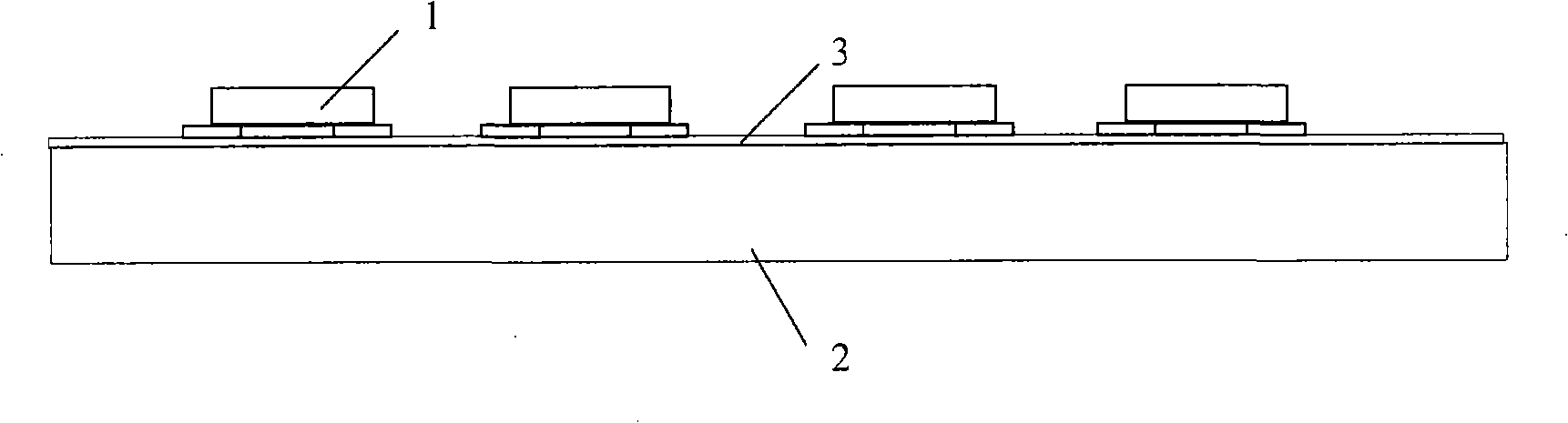
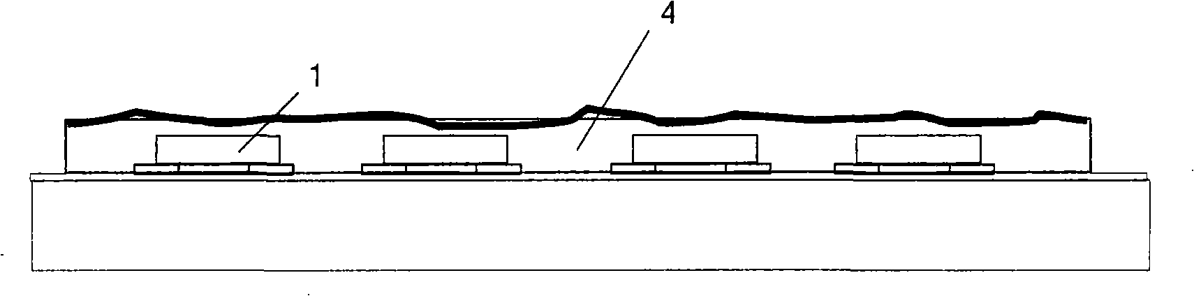
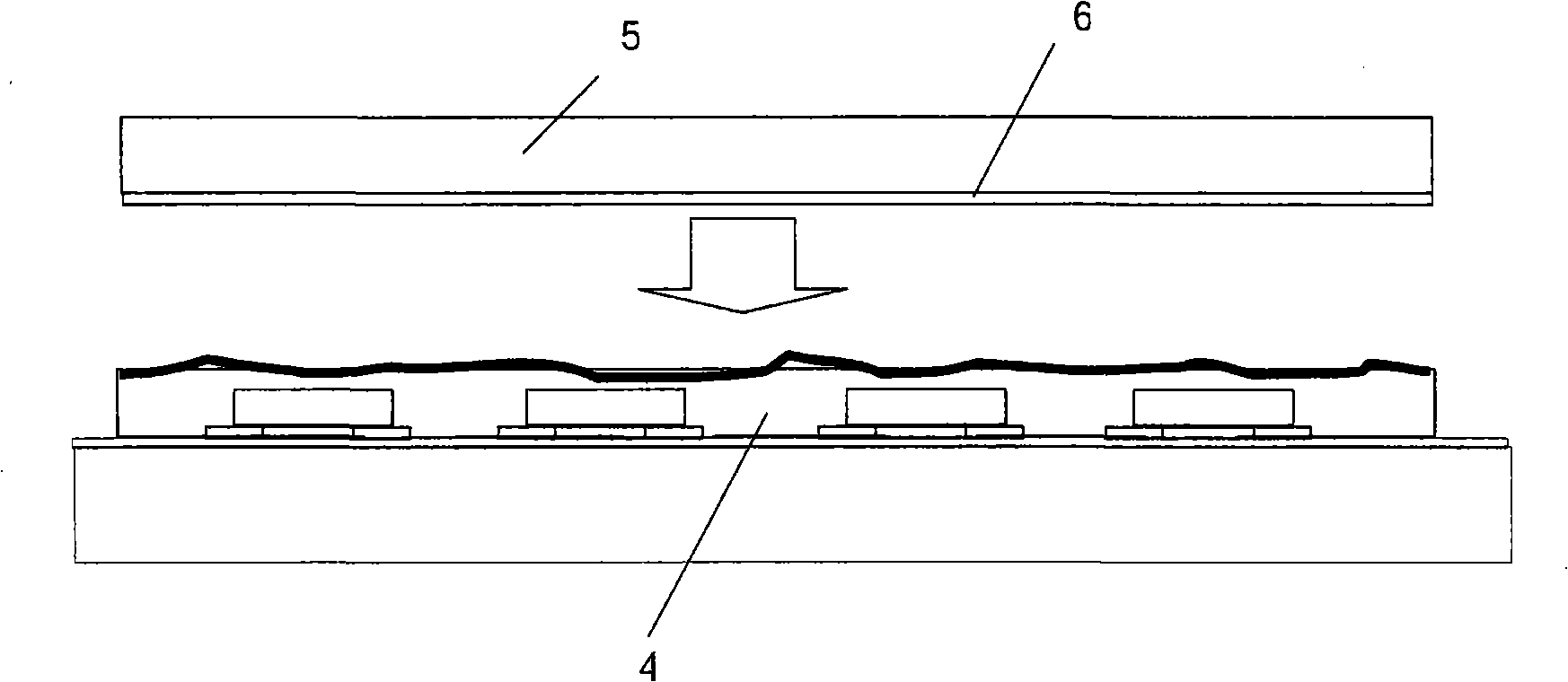
[0041] The invention discloses a flat plate / wafer structure packaging method. Such as figure 1 It is shown that the cut crystal grain 1 is redistributed on the redistribution tool 2 through the pick-up and placement and precise alignment system; wherein the lower substrate 2 of the redistribution tool includes a first separation layer 3 with an alignment pattern, forming On it, the crystal grain 1 is fixed on the first separation layer 3 with a p...


PUM


Abstract

The present invention provides an apparatus and a method for panel / wafer molding. The present invention discloses a base with a first separation layer, an upper molding base with a second separation layer, a cheap molding layer and a vacuum panel bonding machine for bonding, a curing unit, a cleaning unit and a separating unit; wherein upper molding base is rectangular or round. Therefore the present invention providing a simple, cheap universal panel / wafer molding apparatus for a round or rectangular type panel, and does no harm to the chip active surface.

Description

technical field [0001] The present invention relates to a flat-panel / wafer structure packaging device and method, more specifically, a simple flat-panel / wafer structure packaging device and method. Background technique [0002] In the field of semiconductor devices, device densities are increasing and device sizes are shrinking. Therefore, the demands on the packaging and interconnection technology of the high-density device are increasing day by day. [0003] Traditional packaging technology must first cut the die on the wafer into individual dies, and then package the dies individually. Therefore, the process of the above-mentioned technology is very time-consuming. Therefore, the chip packaging technology is greatly affected by the development of integrated circuits. Therefore, when the size requirements of electronic devices are increasing, so is the packaging technology. Based on the above factors, the trend of packaging technology is developing in the following dire...

Claims


Application Information

Patent Timeline
Patent Type & Authority Applications(China)
IPC IPC(8): H01L21/56
CPCH01L2924/14H01L2924/01033H01L24/96H01L21/568H01L21/561H01L21/565H01L2924/181H01L2924/3511H01L2924/00
Inventor 杨文焜许献文郑明忠
Owner ADVANCED CHIP ENG TECH INC
Why Eureka
Try Eureka