Active element array substrate
A technology of active components and array substrates, applied in the direction of electrical components, electric solid devices, semiconductor devices, etc., can solve problems such as electrostatic damage to lines, and achieve the effect of reducing the possibility of damage
- Summary
- Abstract
- Description
- Claims
- Application Information
AI Technical Summary
Problems solved by technology
Method used
Image
Examples
no. 1 example
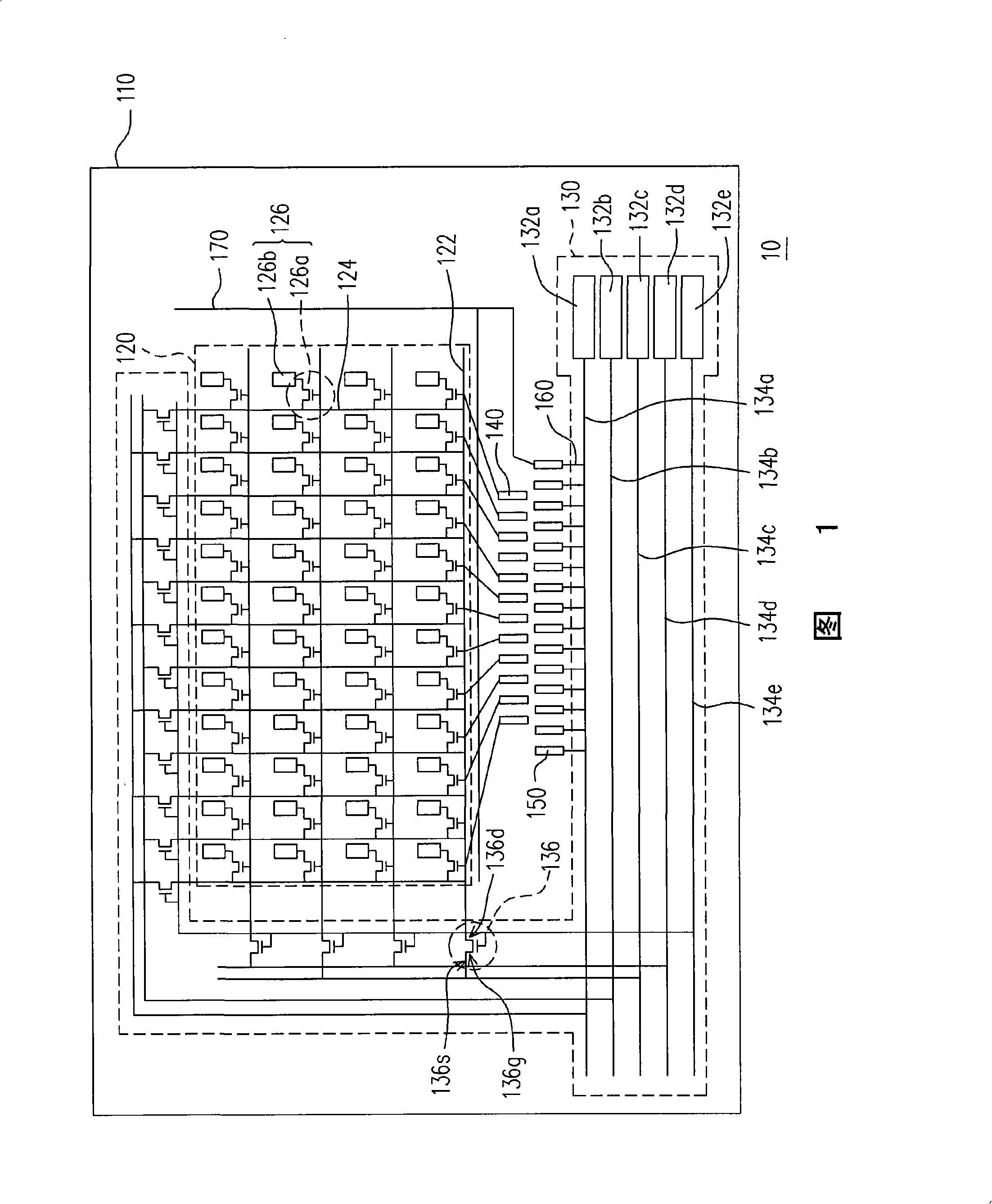
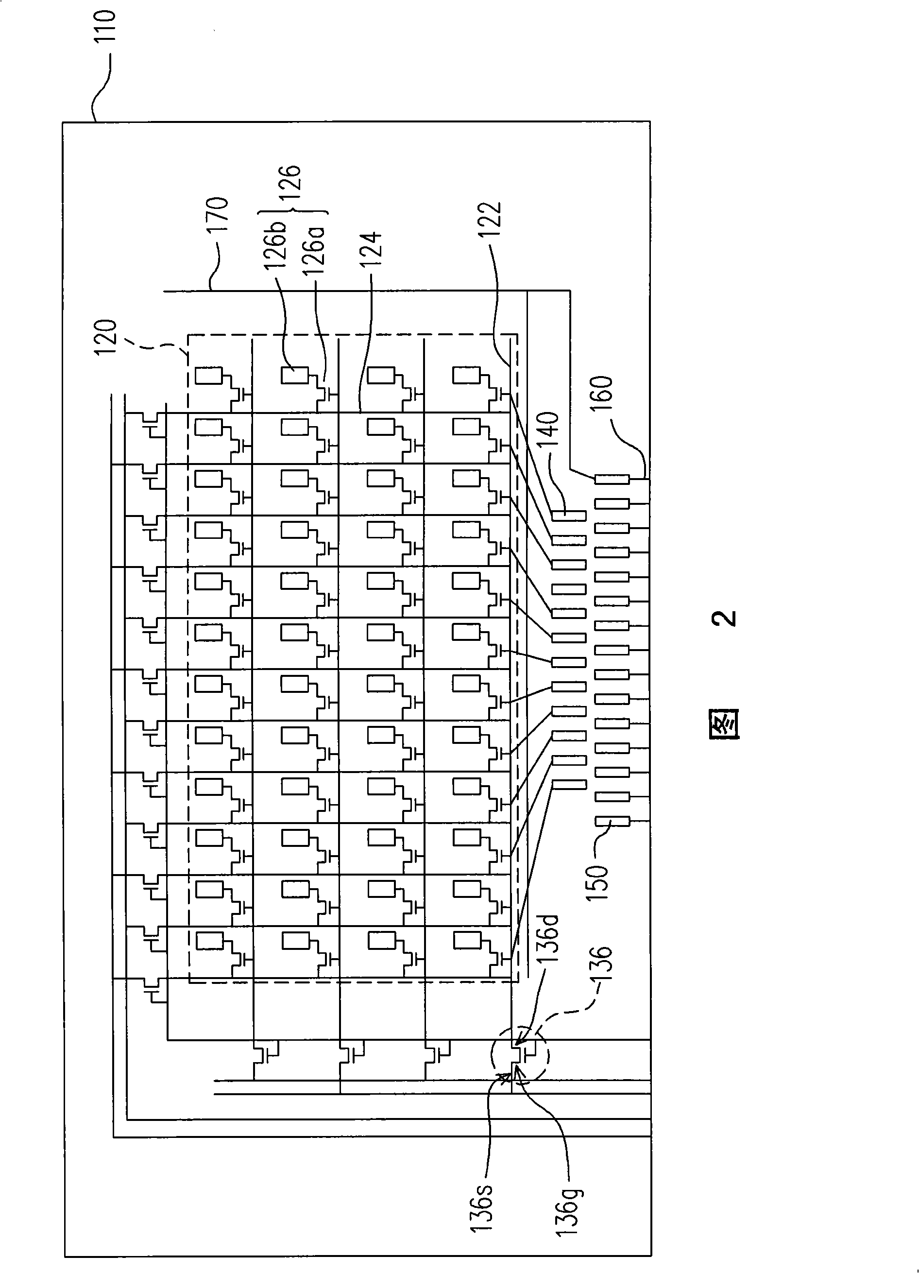
[0024] FIG. 1 is a schematic diagram of an active device array substrate before dicing according to a first embodiment of the present invention. Please refer to FIG. 1, the active element array substrate 10 of this embodiment includes a substrate 110, an active element array 120, a detection circuit 130, a plurality of driver chip pads 140, a plurality of flexible circuit board pads 150, a plurality of The connection wire 160 is connected to an internal electrostatic protection ring 170 , wherein the material of the substrate 110 can be glass, quartz or other transparent materials. The active device array 120 is disposed on the substrate 110, and the active device array 120 includes a plurality of scan lines 122, a plurality of data lines 124 and a plurality of pixel structures 126, wherein each pixel structure 126 uses any scan line 122 and any data Controlled by line 124. In addition, each pixel structure 126 includes an active device 126a and a pixel electrode 126b, wherei...
no. 2 example
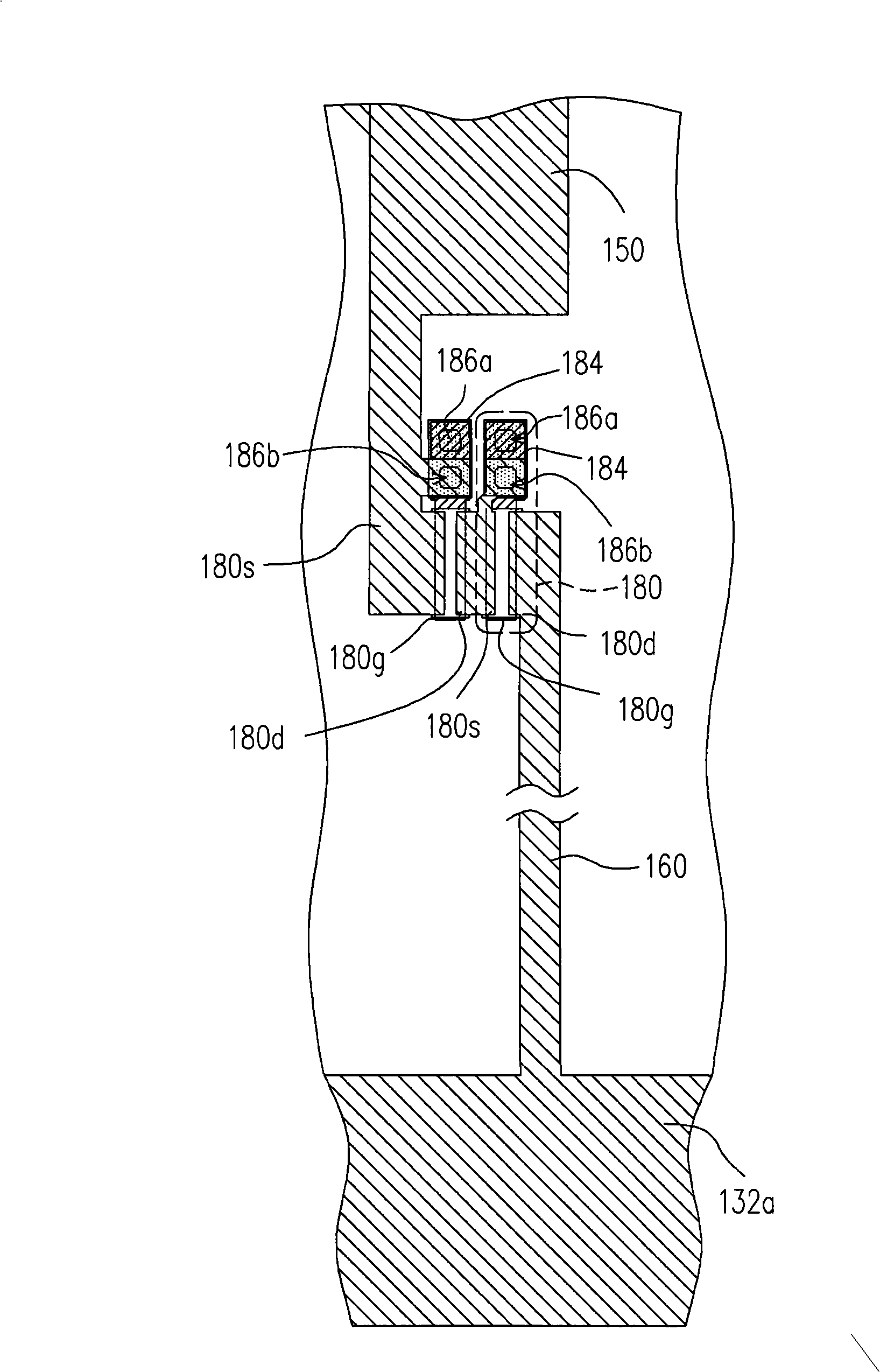
[0032] image 3 It is a partially enlarged view of the active device array substrate before cutting according to the second embodiment of the present invention. Please refer to image 3 , this embodiment is similar to the first embodiment, the difference is that in order to prevent the detection signal from interfering with the operation of the active device array 120, the active device array substrate of this embodiment further includes a plurality of unidirectional switch elements 180, which are arranged on Part of the flexible circuit board pads 150 and the connection lines 160 , and each one-way switch element 180 is connected to the flexible circuit board pads 150 and the connection lines 160 .
[0033] Each one-way switch element 180 includes a gate 180g, a source 180s and a drain 180d, wherein the gate 180g is electrically connected to any flexible printed circuit pad 150 . The source 180s is electrically connected to the gate 180g, and the drain 180d is electrically co...
no. 3 example
[0037] FIG. 5 is a schematic diagram of the active device array substrate before cutting according to the third embodiment of the present invention. Please refer to FIG. 5 , this embodiment is similar to the first embodiment, the difference is that: in the active element array substrate 10' of this embodiment, the substrate 110 is divided into a plurality of panel areas 110a, and the plurality of active elements The arrays 120 are respectively disposed on the panel areas 110a. In addition, some of the FPC pads 150 on each panel area 110 a are electrically connected to the detection circuit 130 via the connecting wire 160 .
[0038] To put it simply, each active device array 120 is electrically connected to the detection circuit 130 via the internal ESD protection ring 170 , the flexible circuit board pad 150 and the connecting wire 160 . Therefore, when the electrostatic discharge occurs, the current can flow into the detection circuit 130 to reduce the possibility of damage ...
PUM
 Abstract
Description
Claims
Application Information
 - R&D
- Intellectual Property
- Life Sciences
- Materials
- Tech Scout
- Unparalleled Data Quality
- Higher Quality Content
- 60% Fewer Hallucinations
Browse by: Latest US Patents, China's latest patents, Technical Efficacy Thesaurus, Application Domain, Technology Topic, Popular Technical Reports.
© 2025 PatSnap. All rights reserved.Legal|Privacy policy|Modern Slavery Act Transparency Statement|Sitemap|About US| Contact US: help@patsnap.com


