Lattice-mismatched semiconductor structures with reduced dislocation defect densities related methods for device fabrication

A lattice mismatch, semiconductor technology, applied in semiconductor/solid-state device manufacturing, semiconductor devices, electrical components, etc.

Active Publication Date: 2008-11-05
TAIWAN SEMICON MFG CO LTD
View PDF3 Cites 36 Cited by
  • Summary
  • Abstract
  • Description
  • Claims
  • Application Information

AI Technical Summary

Problems solved by technology

However, an important limitation of epitaxial necks is the size of the area to be applied

Method used


Image

  • Lattice-mismatched semiconductor structures with reduced dislocation defect densities related methods for device fabrication
  • Lattice-mismatched semiconductor structures with reduced dislocation defect densities related methods for device fabrication
  • Lattice-mismatched semiconductor structures with reduced dislocation defect densities related methods for device fabrication

Examples


Embodiment Construction

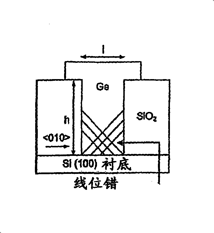
[0046] According to various embodiments of the invention, the present invention is concerned with the fabrication of monolithic lattice-mismatched semiconductor heterostructures with limited area regions of the upper surface substantially depleted of line dislocations and other dislocation defects , and the fabrication of semiconductor devices based on such lattice-mismatched heterostructures.

[0047] Silicon (Si) is considered to be the most common semiconductor used in the electronics industry today. Most of the silicon used to form wafers is formed from single crystal silicon. Silicon wafers are used as substrates on which CMOS devices are formed. A silicon wafer also refers to a semiconductor substrate or a semiconductor wafer. However, although described in connection with silicon wafers, substrates comprising or consisting essentially of other semiconductor materials are also contemplated without departing from the spirit and scope of the present invention.

[0048] ...


PUM


Abstract

Fabrication of monolithic lattice-mismatched semiconductor heterostructures with limited area regions having upper portions substantially exhausted of threading dislocations, as well as fabrication of semiconductor devices based on such lattice-mismatched heterostructures.

Description

[0001] Cross References to Related Applications [0002] This application claims priority to US Provisional Patent Application No. 60 / 681,940, filed May 17, 2005, the entire disclosure of which is incorporated herein by reference. technical field [0003] The present invention relates to lattice mismatched semiconductor heterostructures, and more particularly to selective channel material regrowth associated with integration of dissimilar semiconductor materials. Background technique [0004] As the operating speed and computing power of microelectronic devices increase, there is a demand for increasing the complexity and functionality of semiconductor structures used to manufacture the devices. The heterogeneous integration of dissimilar semiconductor materials, such as III-V materials such as gallium arsenide, gallium nitride, indium aluminum arsenide and / or germanium with silicon or silicon germanium substrates, is important for increasing the functionality and performanc...

Claims


Application Information

Patent Timeline
Patent Type & Authority Applications(China)
IPC IPC(8): H01L21/20
CPCH01L21/02647H01L21/02381H01L21/0245H01L21/0251H01L21/02521H01L21/02532H01L21/0254H01L21/02639H01L21/7624H01L21/8258H01L29/66795H01L29/785H01L21/20
Inventor 安东尼·J·洛赫特费尔德马修·T·柯里程志渊詹姆斯·菲奥里扎格林·布雷恩维特托马斯·A·郎杜
Owner TAIWAN SEMICON MFG CO LTD
Why Eureka
Try Eureka