Semiconductor device

A semiconductor and conductor technology, applied in the field of semiconductor devices with photoelectric conversion function, can solve problems such as loss of transparency of sealing resin, and achieve the effect of avoiding cracking of sealing resin and preventing peeling

Inactive Publication Date: 2008-12-03
RENESAS ELECTRONICS CORP
View PDF1 Cites 2 Cited by
  • Summary
  • Abstract
  • Description
  • Claims
  • Application Information

AI Technical Summary

Problems solved by technology

However, when the sealing resin contains a lot of fillers, the transparency of the sealing resin will be lost

Method used


Image

  • Semiconductor device
  • Semiconductor device
  • Semiconductor device

Examples


Embodiment Construction

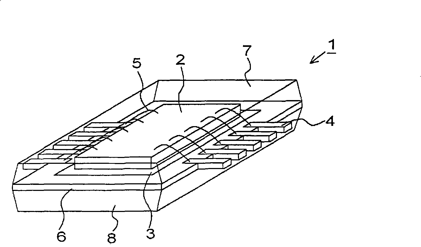
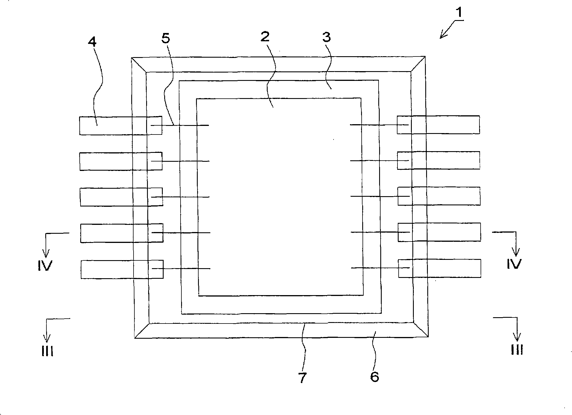
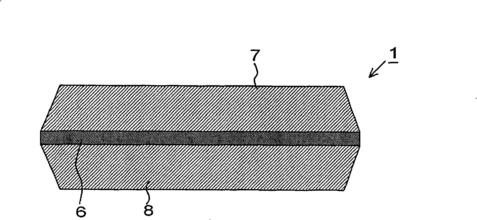
[0019] The semiconductor device according to the first embodiment of the present invention will be described. figure 1 A schematic perspective view showing a semiconductor device according to the first embodiment of the present invention, figure 2 Indicates a schematic top view. and, image 3 express figure 2 A schematic sectional view of the line III-III, Figure 4 express figure 2 A schematic sectional view of line IV-IV.

[0020] The semiconductor device 1 includes a semiconductor element 2 having a photoelectric conversion function, a conductor electrically connected to the semiconductor element 2 , and a sealing resin for sealing them. The conductor includes, for example, an island pad 3 on which a semiconductor element 2 is mounted and electrically connected to the semiconductor element 2 , and a wire 4 electrically connected to the semiconductor element 2 via a bonding wire 5 . Furthermore, in the semiconductor device 1 , the semiconductor element 2 and the lik...


PUM


Abstract

A semiconductor device comprises a semiconductor chip having a photoelectric conversion function and conductor connecting with the semiconductor chip electrically. The semiconductor chip is sealed by resin. The resin comprises a first sealing resin, second sealing resin and third sealing resin. The second sealing resin has transparency for optical signal to the semiconductor chip and seals one side of the conductor. The third sealing resin seals the other side of the conductor and has a linear thermal expansion coefficient and thickness which may restrain at least a part of flexion of the conductor caused by the linear thermal expansion of the second sealing resin.; The first sealing resin seals at least a part of the conductor, is sandwiched between the second sealing resin and the third sealing resin, and has a linear thermal expansion coefficient which may restrain at least a part of the linear thermal expansion of the second sealing resin.

Description

technical field [0001] The present invention relates to a semiconductor device, in particular to a semiconductor device with a photoelectric conversion function. Background technique [0002] In semiconductor devices, semiconductor elements, wiring, and the like are generally sealed with resin to protect them from external environments. The sealing resin generally uses a material containing a filler (glass or the like made into fine particles). However, when the sealing resin contains a lot of fillers, the transparency of the sealing resin will be lost. Therefore, when sealing a semiconductor element having a photoelectric conversion function, it is necessary to transmit and receive light between the inside and outside of the semiconductor device without scattering light, and therefore, a transparent sealing resin containing no filler is used for resin sealing. [0003] For example, in the optical module described in Patent Document 1, the optical element and the wiring bo...

Claims


Application Information

Patent Timeline
Patent Type & Authority Applications(China)
IPC IPC(8): H01L23/28H01L23/29H01L23/31H01L31/0203H01L33/00H01L33/54H01L33/62
CPCH01L24/49H01L31/0203H01L23/3135H01L23/49558H01L2924/01079H01L24/48H01L2224/48091H01L33/52H01L2224/49175H01L2224/48247H01L24/45H01L2224/45144H01L2924/00014H01L2924/181H01L2924/00H01L2924/00012H01L2224/45015H01L2924/207
Inventor 中泽大望
Owner RENESAS ELECTRONICS CORP
Why Eureka
Try Eureka