Manufacturing method for n type SiC semiconductor device ohmic contact

A manufacturing method and ohmic contact technology, applied in the field of microelectronics, can solve the problems of poor ohmic contact interface matching and high ohmic contact annealing temperature, and achieve the effect of avoiding matching problems and reducing contact barriers.

Inactive Publication Date: 2008-12-31
XIDIAN UNIV
View PDF0 Cites 12 Cited by
  • Summary
  • Abstract
  • Description
  • Claims
  • Application Information

AI Technical Summary

Problems solved by technology

[0007] The purpose of the present invention is to propose a method for making ohmic contacts of n-type SiC materials, to overcome the problems of high annealing temperature for making ohmic contacts a

Method used


Image

  • Manufacturing method for n type SiC semiconductor device ohmic contact
  • Manufacturing method for n type SiC semiconductor device ohmic contact
  • Manufacturing method for n type SiC semiconductor device ohmic contact

Examples


Embodiment Construction

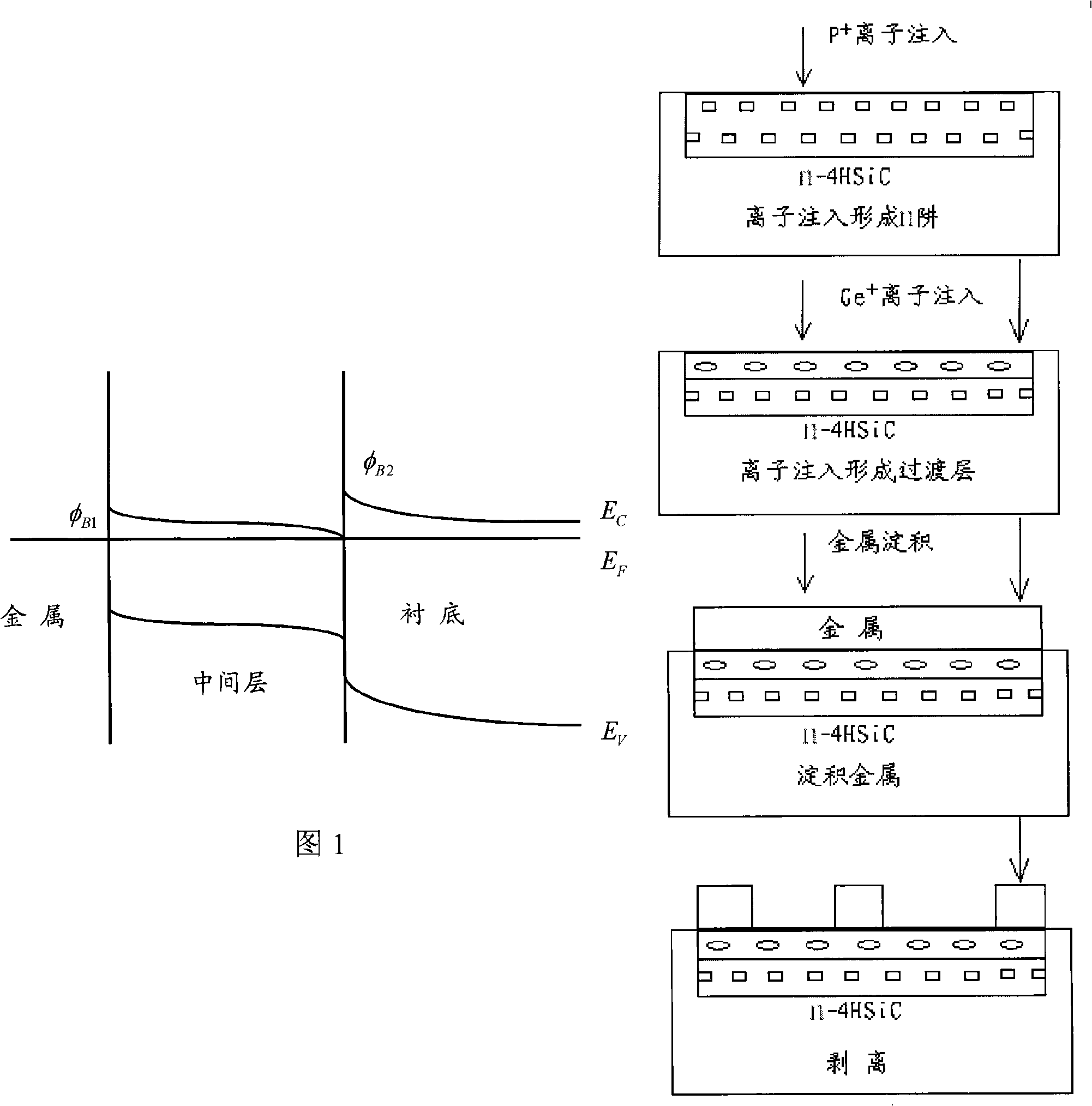
[0020] refer to figure 2 , the substrate used in the present invention is an n-type 4H-SiC substrate, and the thickness of one layer on the substrate is 5 μm, and the doping concentration Na=7.4×10 16 cm -3 The p-type 4H-SiC epitaxial layer, the ohmic contact fabrication process is as follows:

[0021] Step 1, pretreat the n-type 4H-SiC substrate, and implant the epitaxial layer with a concentration of 1×10 20 cm -3 P + ions, forming an n-well.

[0022] First, when the temperature is 550±5℃, the energy is 100keV, the dose is 8.3×10 14 cm -2 ;P + Ions were implanted into the epitaxial layer of the n-type 4H-SiC substrate.

[0023] Then, when the temperature is 550±5℃, the energy is 50keV, and the dose is 2.5×10 15 cm -2 . P + Ions were implanted on the epitaxial layer of the n-type 4H-SiC substrate to form a concentration of 1×10 20 cm -3 The n-well.

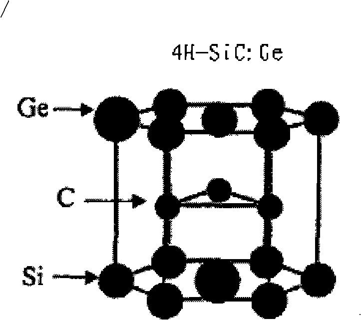
[0024] Step 2, the implantation concentration on the 4H-SiC material forming the n well is at least 10 21 cm -...


PUM


Abstract

The invention discloses an Ohmic contact preparation method for a n-typed SiC semiconductor unit, which mainly solves the problems that the Ohmic contact annealing temperature of the n-typed SiC material is high and poor match is existing in the interface. The process of the method comprises the following steps: a substrate of the n-typed SiC is pretreated, and P<+> ion is implanted to the substrate of the n-typed SiC twice to form n-traps; the n-traps are implanted by Ge<+> ion for four times to form a SiC:Ge mesosphere which is annealed under the protection of C membrane, metal is deposited on the annealed mesosphere of the SiC:Ge, then an electrode zone is defined and an electrode is prepared. The method of the invention has the advantages of low annealing temperature, being lower than the contact resistance and the square resistance, and can be applied to the Ohmic contact preparation of n-typed SiC semiconductor units.

Description

technical field [0001] The invention belongs to the technical field of microelectronics and relates to the manufacture of semiconductor materials, in particular to a method for manufacturing ohmic contacts of n-type SiC semiconductor materials. Background technique [0002] At present, the development of SiC devices has become a research hotspot in the field of semiconductor device circuits. Ohmic contact is an important process in the preparation of SiC devices. In high temperature and high power applications, the low specific contact resistance and high stability of ohmic contact are two important factors that determine the performance of the device. In the working state of high current density, a small resistance will cause a large voltage drop, and the thermal stability of the ohmic contact ratio contact resistance at high temperature is an inevitable factor to be considered, otherwise the degradation of the ohmic contact will lead to changes in the performance of the en...

Claims


Application Information

Patent Timeline
IPC IPC(8): H01L21/28
Inventor 郭辉张玉明程萍张义门陈达
Owner XIDIAN UNIV
Why Eureka
Try Eureka