Semiconductor package and manufacturing method thereof

A semiconductor and packaging technology, applied in the field of semiconductor packaging and its manufacturing method, can solve problems such as delamination and limited adhesion

Inactive Publication Date: 2008-12-31
SILICONWARE PRECISION IND CO LTD
View PDF6 Cites 22 Cited by
  • Summary
  • Abstract
  • Description
  • Claims
  • Application Information

AI Technical Summary

Problems solved by technology

In addition, since the metal pad is an electroplated layer with a thickness of about 0.5 to 5 μm, and it is only in contact with the encapsulant at the bottom of the groove, the mutual adhesion is obviously limited. Delamination (delamination) D occurs, such as Figure 3B shown

Method used


Image

  • Semiconductor package and manufacturing method thereof
  • Semiconductor package and manufacturing method thereof
  • Semiconductor package and manufacturing method thereof

Examples


no. 1 example

[0054] see Figure 4A to Figure 4G , is a schematic cross-sectional view of the first embodiment of the semiconductor package and its manufacturing method of the present invention.

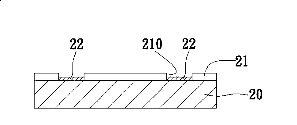
[0055] Such as Figure 4A As shown, at first, prepare a carrier plate 40 (for example, copper plate (CuPlate)) of a metal material, and cover the first resistance layer 41 on a surface of the metal carrier plate 40, and make the first resistance layer 41 form how many times A first opening 410 is used to define a subsequent terminal position 41a for electrical connection with the semiconductor chip and a die pad position 41b for placing the semiconductor chip.

[0056] Such as Figure 4B As shown, an electroplating process is performed to form a metal block 42 in the first opening 410 by electroplating, and its material is copper, for example.

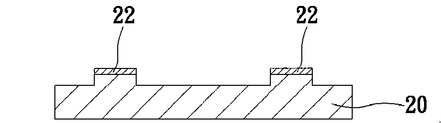
[0057] Such as Figure 4C As shown, the first resistance layer 41 is removed, and the second resistance layer 43 is covered on the metal carrier 40, a...

no. 2 example

[0067] see Figure 5A to Figure 5G , is a schematic diagram of a second embodiment of the semiconductor package and its manufacturing method of the present invention. The semiconductor package and its manufacturing method of this embodiment are roughly the same as those of the foregoing embodiments, the main difference being that when forming a metal block on the metal carrier, the metal block is in the shape of multiple columns, and a metal layer covering the multiple columns is formed. The metal layer on the outer surface of the block, so that when the metal carrier and the metal block are subsequently removed, a groove with a protruding metal layer can be formed on the surface of the encapsulant, thereby increasing the number of conductive elements subsequently planted in the groove The contact area and bonding force with the metal layer.

[0068] Such as Figure 5A As shown, a metal carrier 50 is prepared, and a first resistance layer 51 is covered on a surface of the me...

no. 3 example

[0076] see again Figure 6 , is a schematic diagram of the third embodiment of the semiconductor package of the present invention.

[0077]The semiconductor package of this embodiment is substantially the same as the previous embodiment, the main difference is that after the metal block is formed on the metal carrier, when the metal layer covering the metal block is to be formed, the second resistive layer is added compared with the previous embodiment. Two opening sizes, so as to form a metal layer 64 covering the metal block on the metal carrier, and at the same time form an extension part 640, for subsequent completion of chip placement, wire bonding, packaging and molding operations, and remove the metal carrier and the metal block, the metal layer 64 can be formed on the bottom surface and the side of the groove 670 on the surface of the encapsulant 67, and the metal layer extension 640 can be formed on the surface of the encapsulant 67 around the groove 670, thereby incr...


PUM


Abstract

The invention discloses a semi-conductor packaging unit and a manufacturing method hereof, which provides a carrier plate, wherein, a plurality of metal blocks and a metallic layer for coating the metal blocks are formed on the carrier plate so as to electrically connect at least one semi-conductor to the metallic layer, and then a packaging colloid coating the semi-conductor chip is also formed on the metallic carrier plate, then, the carrier plate and the metal blocks are removed to form a plurality of grooves on the surface of the packaging colloid correspondingly. At the bottom surface and the side of the grooves are covered with a metallic layer so as to lead the conductive elements to be effectively positioned in the grooves and fully conjugated with the metallic layer.

Description

technical field [0001] The invention relates to a semiconductor package and its manufacturing method, in particular to a semiconductor package without a carrier and its manufacturing method. Background technique [0002] There are many types and types of traditional semiconductor packages that use lead frames as chip carriers. As far as Quad Flat Non-leaded (QFN) semiconductor packages are concerned, they are characterized in that no external leads are provided. That is, there is no external pin for electrical connection with the outside as in the existing quad flatpackage (QFP) semiconductor package, so that the size of the semiconductor package can be reduced. [0003] However, with the development trend of thinner and smaller semiconductor products, the traditional QFN package with lead frame is often unable to further reduce the overall height of the package due to the limitation of the thickness of the encapsulant. Therefore, the industry has developed a carrierless (ca...

Claims


Application Information

Patent Timeline
Patent Type & Authority Applications(China)
IPC IPC(8): H01L21/50H01L21/60H01L21/56H01L23/488H01L23/31
CPCH01L2224/48091H01L2224/73265H01L2924/15311H01L2924/3025H01L2924/00014H01L2924/00
Inventor 李春源洪孝仁林宥纬张锦煌赖正渊
Owner SILICONWARE PRECISION IND CO LTD
Why Eureka
Try Eureka