Check patentability & draft patents in minutes with Patsnap Eureka AI!

Cmp method of semiconductor device

A semiconductor and device technology, applied in the field of semiconductor devices, can solve problems such as irregular tungsten films, particle residues, process abnormalities, etc.

Inactive Publication Date: 2008-12-31
SK HYNIX INC
View PDF1 Cites 3 Cited by
  • Summary
  • Abstract
  • Description
  • Claims
  • Application Information

AI Technical Summary

Problems solved by technology

At this time, the tungsten film remained irregular at the edge of the wafer because the pad pressure was not constant near the edge of the wafer (i.e., about 10 mm from the edge) where contact between the polishing pad and the wafer was insufficient
If a subsequent process of deposition or etching of an oxide film or a nitride film having a large film stress or a subsequent thermal process is performed in this state, process abnormalities such as lifting may occur due to irregularly held tungsten. ), particle residue and arching

Method used


Image

  • Cmp method of semiconductor device
  • Cmp method of semiconductor device
  • Cmp method of semiconductor device

Examples


Embodiment Construction

[0022] Specific embodiments according to the present invention will now be described with reference to the accompanying drawings.

[0023] However, the present invention is not limited to the disclosed embodiments, but can be implemented in various ways. The embodiments are provided to complete the disclosure of the present invention and to enable those skilled in the art to understand the scope of the present invention. The invention is defined by the claims.

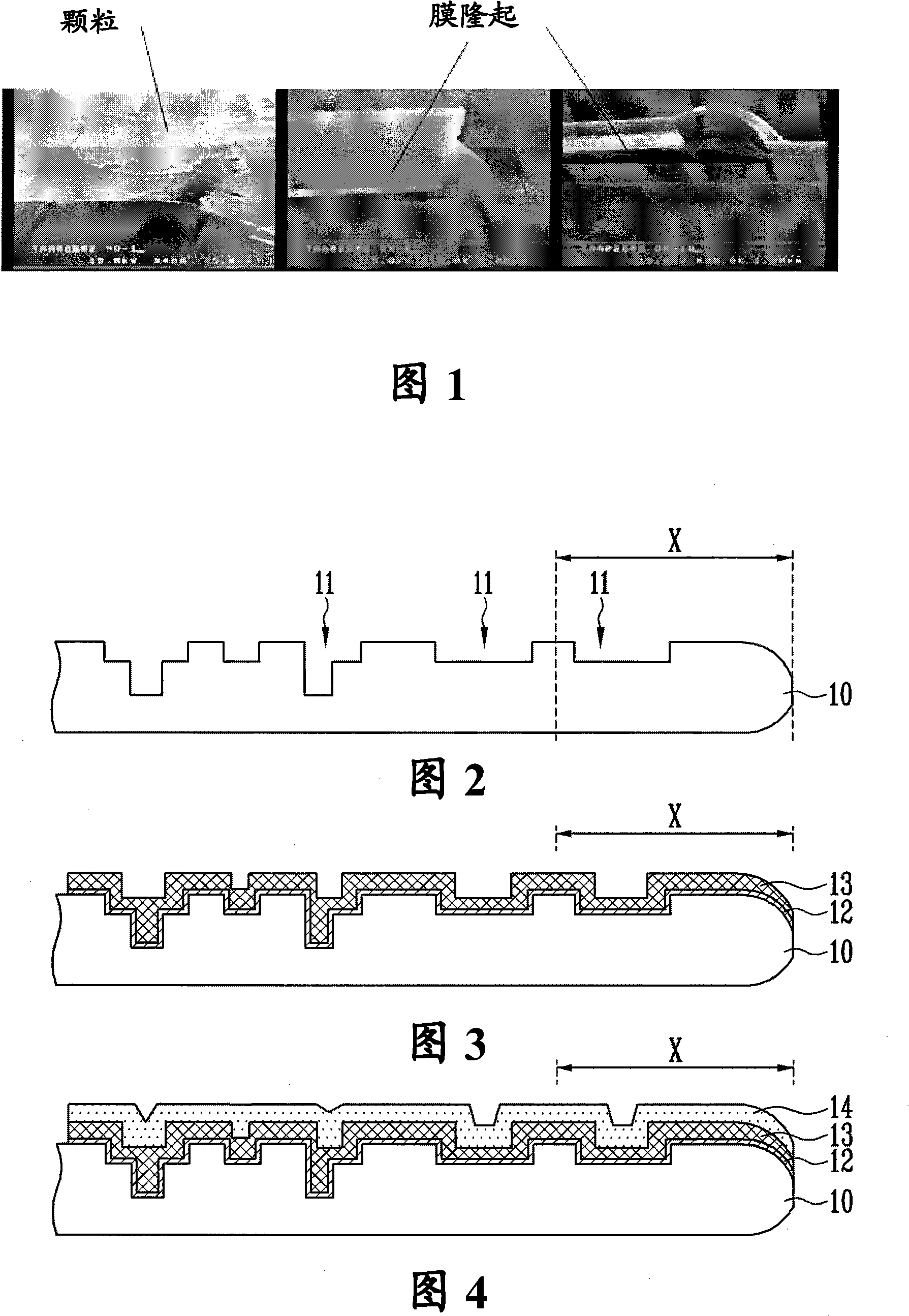
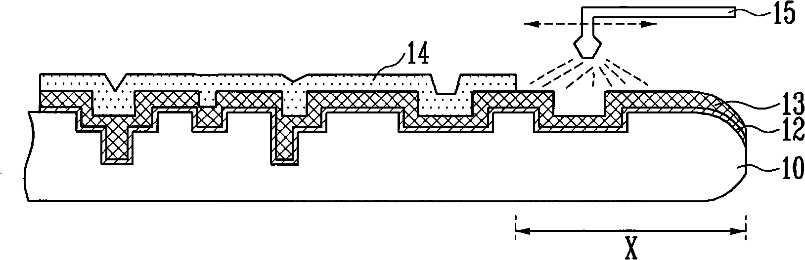
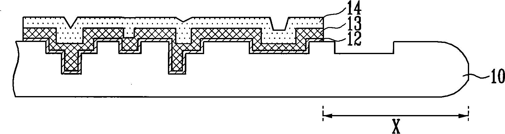
[0024] 2 to 8 are cross-sectional views illustrating a CMP method of a semiconductor device according to an embodiment of the present invention.

[0025] Embodiments of the present invention are explained by taking a metal line forming method using a damascene process as an example.

[0026] Referring to FIG. 2, a damascene pattern 11 for forming a metal line is formed by etching a semiconductor substrate 10 in which an insulating film is formed. The damascene pattern 11 may be formed by forming a hard mask pattern ...


PUM


Abstract

The present invention relates to a Chemical Mechanical Polishing (CMP) method of a semiconductor device. According to the method, a metal layer is formed over a semiconductor substrate in which an edge region define. A passivation layer is formed on the metal layer. The passivation layer formed in the edge region is etched in order to expose the metal layer. The exposed metal layer is removed through etching. The metal layer is polished by performing a CMP process, thus forming a metal line.

Description

[0001] Cross References to Related Applications [0002] This application claims priority from Korean Patent Application No. 10-2007-64486 filed on June 28, 2007, the entire contents of which are incorporated herein by reference. technical field [0003] The present invention relates to semiconductor devices, and more particularly to chemical mechanical polishing (CMP) methods that can remove residues remaining on edge regions of wafers. Background technique [0004] The CMP method is a polishing process in which a chemical reaction by a slurry and a mechanical treatment by a polishing pad are simultaneously performed. Compared with reflow process, etch-back process, etc., which are commonly used for surface planarization, this CMP method is advantageous in that overall polishing can be performed and can also be performed at low temperature. [0005] Specifically, the CMP method is proposed as a polishing process, but recently it is also used as an insulating film etching p...

Claims


Application Information

Patent Timeline
Patent Type & Authority Applications(China)
IPC IPC(8): H01L21/768
CPCH01L21/3212H01L21/32139H01L21/304
Inventor 金兑京赵直镐
Owner SK HYNIX INC
Features
  • R&D
  • Intellectual Property
  • Life Sciences
  • Materials
  • Tech Scout
  • Unparalleled Data Quality
  • Higher Quality Content
  • 60% Fewer Hallucinations
Learn More