Semiconductor device

A semiconductor and device technology, applied in the field of seal ring construction, can solve the problems of reduced strength, increased seal ring stress, and inability to fully utilize the seal ring, and achieve the effects of preventing damage and improving stress tolerance

Inactive Publication Date: 2009-01-07
LAPIS SEMICON CO LTD
View PDF2 Cites 10 Cited by
  • Summary
  • Abstract
  • Description
  • Claims
  • Application Information

AI Technical Summary

Problems solved by technology

That is, the seal ring prevents local stress generated near the scribe line from propagating to the inside of the chip during scribing. However, since the strength of the low-k film near the seal ring decreases, the stress added to the seal ring itself Increase
As a result, the seal ring cannot withstand the stress and is partially damaged or cracked (crack), so that the function as the seal ring cannot be fully exerted.
As a result, impurities such as water are allowed to seep into the interior of the active region, leading to performance degradation

Method used


Image

  • Semiconductor device
  • Semiconductor device
  • Semiconductor device

Examples


Embodiment 1

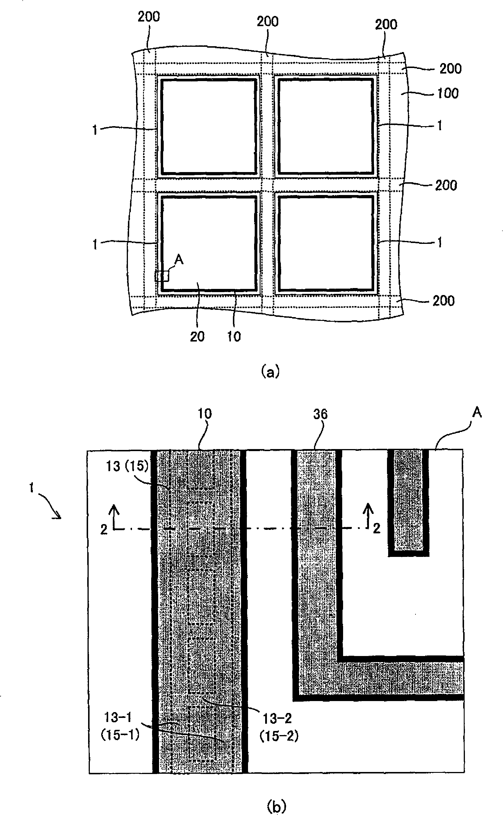
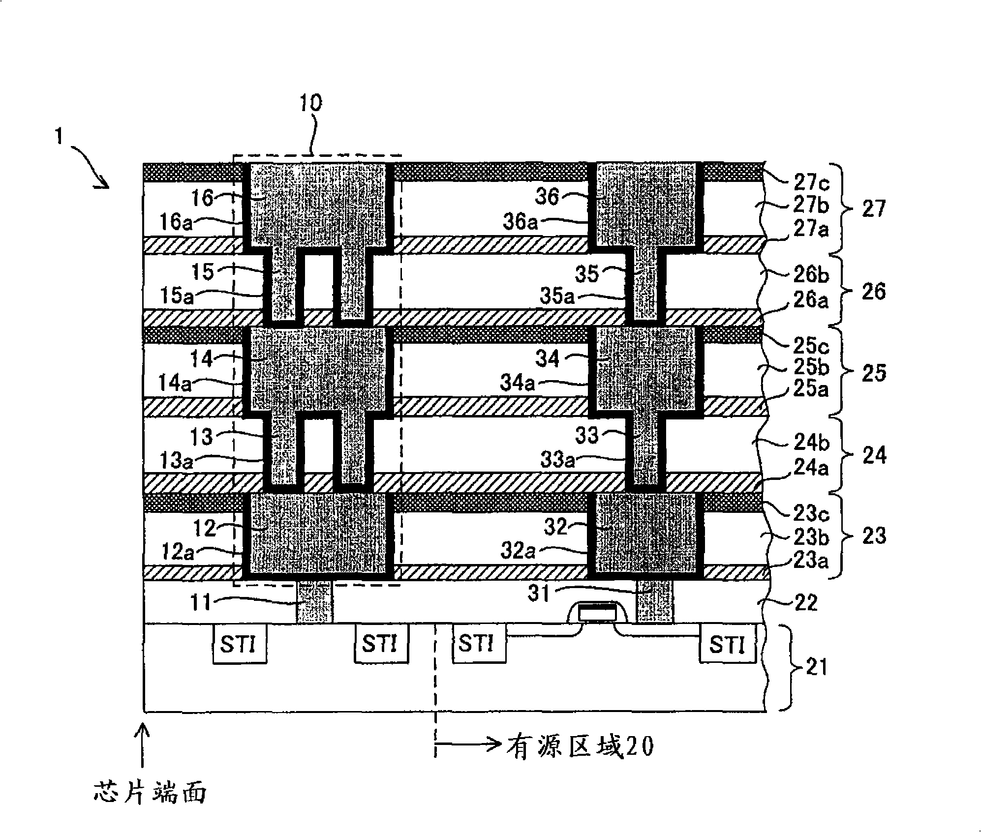
[0023] figure 1 (a) is a plan view showing a part of the wafer 100 on which the semiconductor device 1 according to the first embodiment of the present invention is formed. Scribing lines 200 serving as dicing areas during dicing are provided in a grid pattern on the wafer 100 , and the semiconductor device 1 is diced into individual chips by dicing along the scribing lines 200 . In the semiconductor device 1 , a seal ring 10 is formed in the vicinity of a scribe line 200 formed to surround the periphery thereof. That is, the seal ring 10 is formed near the end face of the chip-diced semiconductor device 1 , and is formed in a cylindrical shape so as to surround the active region 20 in which the circuit portion is formed. As a result, the seal ring 10 can prevent the local stress generated near the end face of the chip from propagating to the active region 20 when dicing or the like is performed.

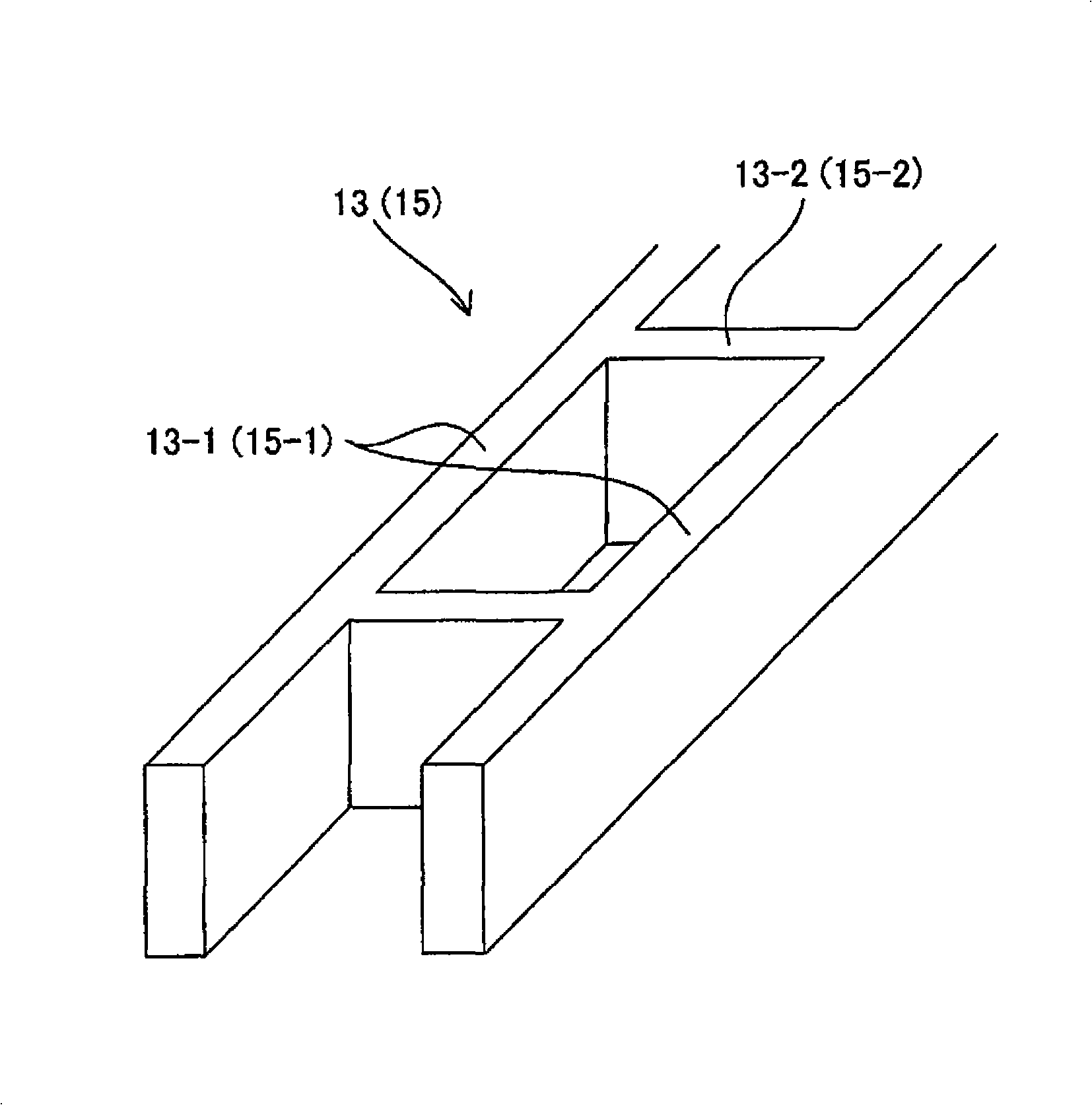
[0024] figure 1 (b) is figure 1 An enlarged view of the area A enclosed by ...

Embodiment 2

[0041] Next, the structure of the semiconductor device 2 according to Embodiment 2 of the present invention will be described with reference to the drawings. The semiconductor device 2 in Embodiment 2 differs from that in Embodiment 1 described above in the configuration of the sealing plug constituting the seal ring. Figure 6 is an enlarged plan view of the sealing ring 50 of the semiconductor device in this embodiment, Figure 7 is along Figure 6 Sectional view of line 7-7. exist Figure 6 In FIG. 2 , as in the above-mentioned first embodiment, the portion where the sealing plug is formed is indicated by a dotted line so that the structure of the internal sealing plug can be understood. Figure 8 It is a perspective view in which only the sealing plug in this embodiment is pulled out. Such as Figure 7 As shown, a sealing plug 53 as a constituent part of the sealing ring 50 in this embodiment is provided in the third interlayer insulating film 24 and connected to the ...


PUM


Abstract

The invention provides a seal ring structure semiconductor device with higher stress resistance. The semiconductor device comprise: a semiconductor layer, including multiple semiconductor elements; a insulated film, disposed on semiconductor layer; a cylinder, running through insulated film and enclosing whole semiconductor element. The cylinder possesses multiple cylinder-shape parallel plugs separating from each other peripherally and multiple walls intersecting with every plug.

Description

technical field [0001] The present invention relates to a semiconductor device, and more particularly to a structure of a seal ring that surrounds the periphery of a semiconductor element and prevents stress from spreading to the inside of the chip. Background technique [0002] With the development of semiconductor devices such as microprocessors and memories, the level of integration of components such as transistors has increased rapidly. Therefore, in order to adapt to the high integration of the substrate level, it is necessary to realize highly integrated multilayer wiring such as wiring. However, conventionally, as the wiring becomes finer, the processing is prolonged, and the signal delay in the wiring layer, that is, the RC delay increases, which hinders the speed-up of the operation speed. Therefore, in order to achieve a higher speed of a microprocessor or the like, it is absolutely necessary to reduce the wiring resistance R and the inter-wiring capacitance C. ...

Claims


Application Information

Patent Timeline
Patent Type & Authority Applications(China)
IPC IPC(8): H01L23/00
CPCH01L23/562H01L2924/0002H01L23/585H01L2924/00H01L21/28H01L21/3205
Inventor 时藤俊一
Owner LAPIS SEMICON CO LTD
Why Eureka
Try Eureka