
Production method of silicon based liquid crystal panel

A manufacturing method and silicon-based liquid crystal technology, applied in nonlinear optics, instruments, optics, etc., can solve problems such as CCD reading misjudgment, uneven slivers, and poor cutting accuracy, so as to improve the yield rate , reduce costs, and improve the accuracy of the method

Inactive Publication Date: 2009-01-14
CHUNGHWA PICTURE TUBES LTD
View PDF0 Cites 6 Cited by
  • Summary
  • Abstract
  • Description
  • Claims
  • Application Information

AI Technical Summary

Problems solved by technology

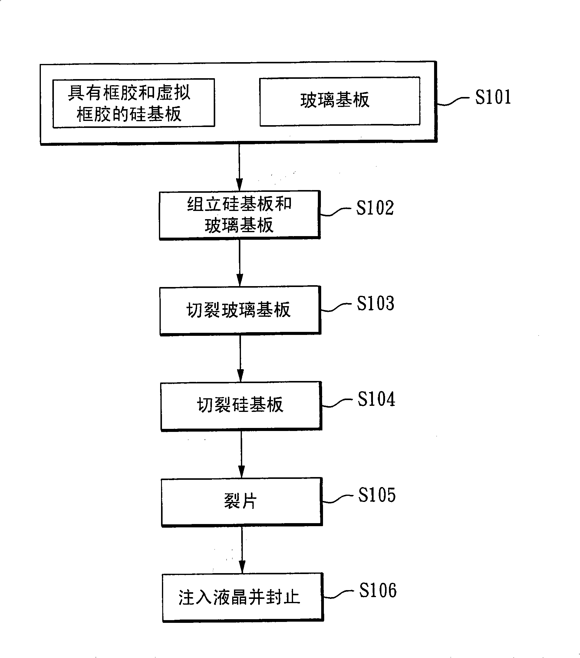
However, there are measurement and cutting errors in the process of generating the alignment edge (for example, the unevenness of the slivers or the wear of the tool), which makes the CCD reading misjudgment, resulting in poor cutting accuracy
Moreover, in addition to the sealant 202 on the silicon substrate 204, a virtual sealant 203 must also be provided to prevent cooling water from penetrating into the panel when the alignment edge is cut, resulting in a waste of sealant

Method used


Image

  • Production method of silicon based liquid crystal panel
  • Production method of silicon based liquid crystal panel
  • Production method of silicon based liquid crystal panel

Examples


Embodiment Construction

[0036] These drawings in the embodiments of the present invention are simplified schematic diagrams. However, these icons only show components related to the present invention, and the components shown are not the actual implementation. The number and shape of the components in the actual implementation are a selective design, and the layout of the components Possibly more complicated.

[0037] see Figure 4 , is a process flow of a method for manufacturing a liquid crystal on silicon panel according to a preferred embodiment of the present invention. Also refer to FIG. 5A to FIG. 5E , which are schematic cross-sectional views of the manufacturing method of the liquid crystal on silicon panel of the present embodiment.

[0038] First, step S401 is performed, providing a silicon substrate 505 (see FIG. 5A ) that has completed the wafer integrated circuit method, and cutting the silicon substrate 505 to form a plurality of silicon chips 506 (see FIG. 5B ). In this embodiment, t...


PUM


Abstract

The invention relates to a manufacturing method used for a silicon-based liquid crystal panel, including the following steps: a glass baseplate provided with a plurality of sealants and a silicon chip provided with a plurality of circuits are provided; the silicon chip and the glass baseplate are combined; the glass baseplate is cut to get a plurality of panel units; and a liquid crystal is injected into the panel units to form the silicon-based liquid crystal panel. With the manufacturing method, the manufacturing accuracy and the defect-free rate of the silicon-based liquid crystal panel can be enhanced.

Description

technical field [0001] The invention relates to a method for manufacturing a liquid crystal on silicon panel (LCoS panel), in particular to a method for manufacturing a liquid crystal on silicon panel suitable for microdisplays. Background technique [0002] Liquid Crystal on Silicon Panel (LCoS panel for short) is a key component of a reflective microdisplay. Its structure is as follows Figure 7 As shown, it mainly includes a silicon chip 701 that has been cut and shaped by the chip integrated circuit method as the lower substrate, a glass substrate 702 with a transparent electrode layer 705 as the upper substrate, and a liquid crystal 703 sandwiched between the two substrates. Moreover, the dislocation portion 704 of the silicon chip 701 that does not overlap with the transparent conductive glass 702 is provided with a pad or a conductive bump (not shown in the figure) for connecting other electronic components. [0003] For a flow chart of an existing LCD-on-Si panel man...

Claims


Application Information

Patent Timeline
Patent Type & Authority Applications(China)
IPC IPC(8): G02F1/1362G02F1/1339
Inventor 刘光华黄莉贞罗宇城莫启能李怀安
Owner CHUNGHWA PICTURE TUBES LTD
Learn More