Electronic package an electronic device

A technology for electronic packaging and electronic devices, applied in circuits, electrical components, electrical solid devices, etc., to achieve the effect of reducing inductance and resistance values, improving power integrity, and improving voltage drop

Active Publication Date: 2009-01-21
MEDIATEK INC
View PDF0 Cites 11 Cited by
  • Summary
  • Abstract
  • Description
  • Claims
  • Application Information

AI Technical Summary

Problems solved by technology

Die Attached to Die Pads

Method used


Image

  • Electronic package an electronic device
  • Electronic package an electronic device
  • Electronic package an electronic device

Examples


Embodiment Construction

[0019] The following descriptions are examples of the present invention. The purpose of this description is to provide a general concept of the present invention and not to limit the scope of the present invention. The scope of protection of the present invention should be defined by the claims. Embodiments of the present invention are described below with reference to the accompanying drawings.

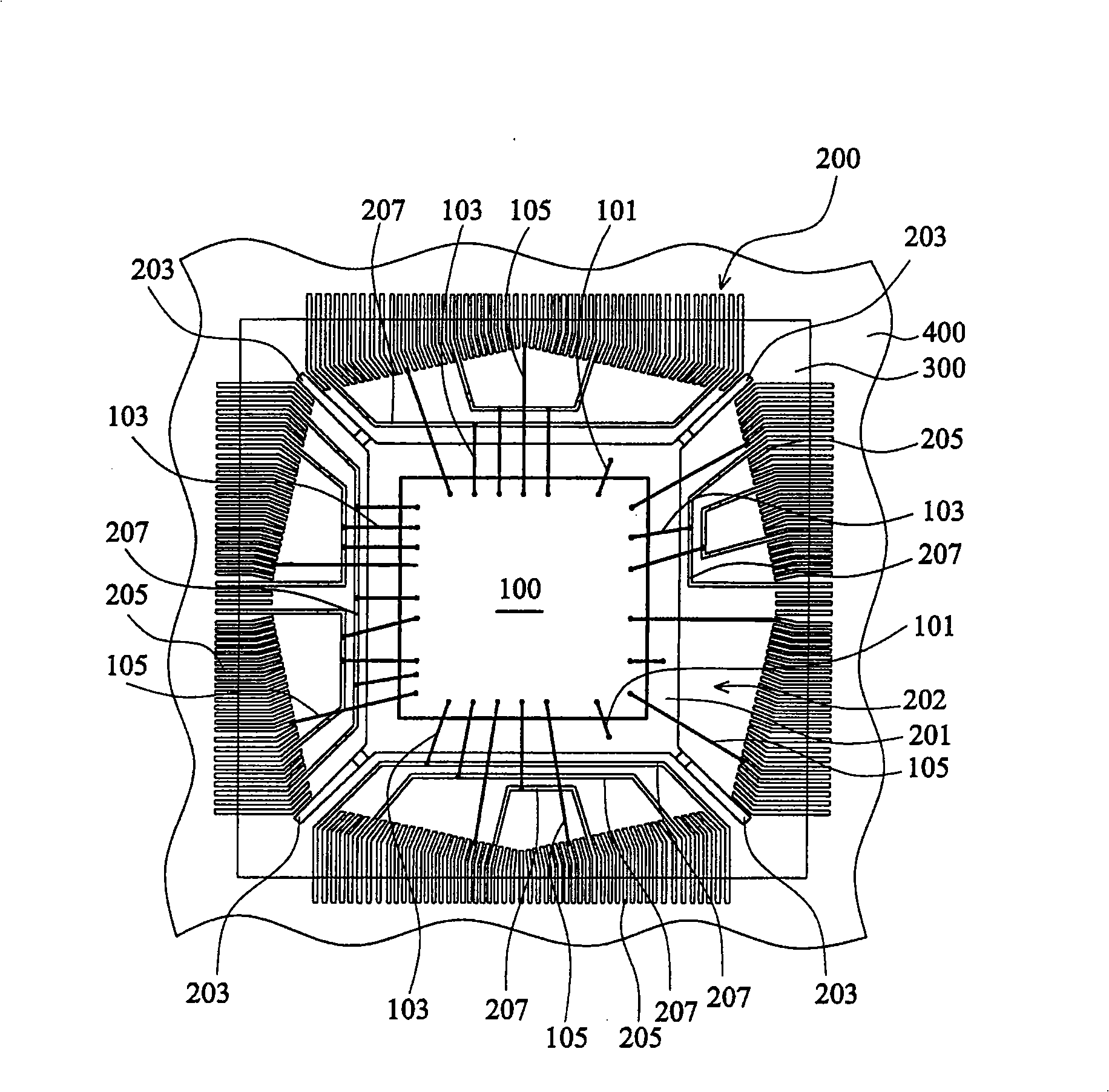
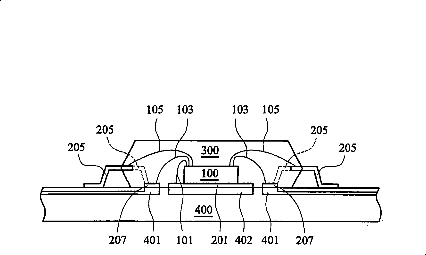
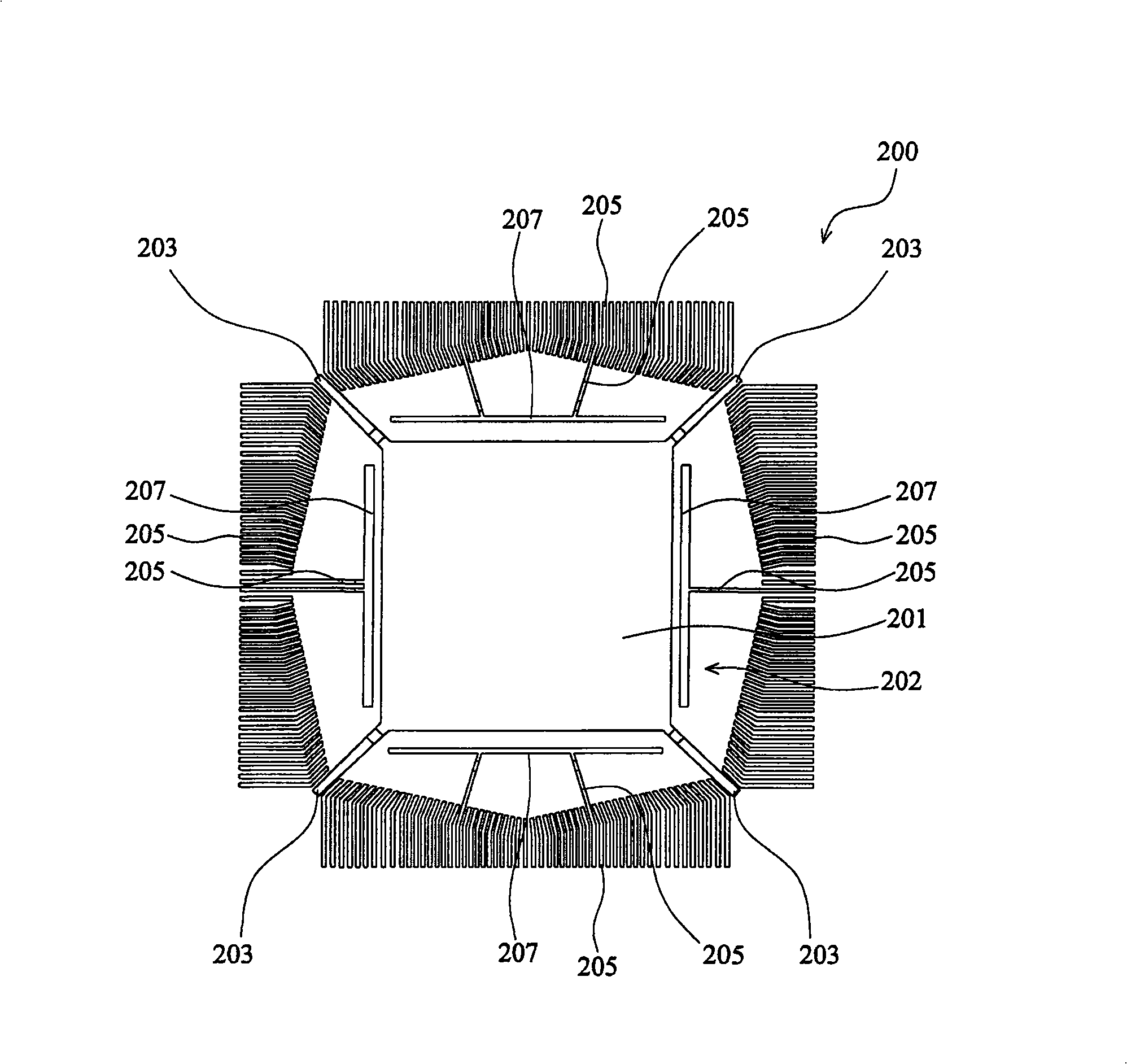
[0020] Please refer to figure 1 and figure 2 ,in figure 1 A schematic plan view of an electronic device with a package according to an embodiment of the present invention is drawn, and figure 2 draw out figure 1 Schematic cross-section of the electronic device. The electronic device includes an electronic package bonded to a circuit board 400 , such as a package substrate or a printed circuit board. In this embodiment, the electronic package is a quad flat package with exposed pads.

[0021] In this embodiment, the electronic package includes: a chip 100 with integrated cir...


PUM


Abstract

The invention discloses an electronic package and an electronic device. The electronic package comprises a die pad, a die, a plurality of leads, a common electrode bar layer, and a molding compound. The die is attached onto the pad. The plurality of leads surrounds the die pad and spaced therefrom to define a ring gap therebetween. The common electrode bar layer is in the ring gap and substantially coplanar to the die pad, in which at least one of the plurality of leads extends to the common electrode bar layer. The molding compound partially encapsulates the die pad and the common electrode bar layer, such that the bottom surfaces of the die pad and the common electrode bar layerare exposed. The invention is capable of reducing inductance and resistance of the circuit, obtaining greater integrity of electric power, improving IR drop problem of the core electric power, and is helpful to high-speed operation and device performance improvement.

Description

technical field [0001] The present invention relates to an electronic package and an electronic device, in particular to an exposed-pad quad flat package (quad flat package, QFP) with a common electrode strip layer and an electronic device with the package. Background technique [0002] Driven by high integration and miniaturization of high-end semiconductor devices, the demand for high-density packaging also increases. To meet the above demands, the semiconductor manufacturing industry must prepare thinner semiconductor packages. In high-integration and high-end semiconductor devices, in order to increase the signal speed, the heat generated by the chip and the inductance in the packaging structure have become problems that cannot be ignored. Therefore, heat dissipation and inductance reduction have become two important tasks in the semiconductor manufacturing industry. Heat generated by the chip can be removed from the packaging structure by providing a thermally conduct...

Claims


Application Information

Patent Timeline
Patent Type & Authority Applications(China)
IPC IPC(8): H01L21/50H01L21/48H01L23/495
CPCH01L23/49541H01L2924/01015H01L2224/4911H01L2924/01082H01L24/48H01L2924/01002H01L23/49551H01L2224/48247H01L2924/19107H01L2924/14H01L2224/49109H01L2924/01033H01L2924/01006H01L2924/01029H01L23/3107H01L2224/48257H01L2224/48091H01L2924/01013H01L2924/30107H01L24/49H01L2924/01077H01L2924/181H01L2924/00014H01L2224/45099H01L2224/05599H01L2924/00012
Inventor 陈南诚陈南璋李锦智
Owner MEDIATEK INC
Why Eureka
Try Eureka