
Optical waveguide device and manufacturing method thereof

A technology for the manufacture of optical waveguides and equipment, which is applied in the directions of optical waveguides and optical waveguides, coupling of optical waveguides, and optical waveguides.

Inactive Publication Date: 2009-01-28
NITTO DENKO CORP
View PDF1 Cites 9 Cited by
  • Summary
  • Abstract
  • Description
  • Claims
  • Application Information

AI Technical Summary

Problems solved by technology

[0004] However, in this type of optical waveguide device, when the above-mentioned light-emitting element 50 is bonded, the adhesive A may overflow and bulge due to pressing the light-emitting element 50 from above or the like, which becomes an obstacle to the optical path.

Method used


Image

  • Optical waveguide device and manufacturing method thereof
  • Optical waveguide device and manufacturing method thereof
  • Optical waveguide device and manufacturing method thereof

Examples


Embodiment

[0042] Forming material of lower cladding layer and upper cladding layer

[0043] 35 parts by weight of 9,9-bis[(4-hydroxyethoxy)phenyl]fluorene diglycidyl ether (ingredient A), 40 parts by weight of 3',4'-epoxy as alicyclic epoxy resin Cyclohexylmethyl-3,4-epoxycyclohexanecarboxylate (manufactured by DAICEL CHEMICALINDUSTRIES, LTD., Celloxide 2021P) (ingredient B), 25 parts by weight of (3',4'-epoxycyclohexane) methyl -3',4'-epoxycyclohexyl carboxylate (manufactured by DAICEL CHEMICAL INDUSTRIES, LTD., Celloxide 2081) (ingredient C), 1 part by weight of 4,4'-bis[bis(β-hydroxyethoxy ) phenylsulfinyl] phenyl sulfide-bis-hexafluoroantimonate 50% propylene carbonate solution (photoacid generator, component D) mixed, thus preparing the lower cladding and surface cladding forming material.

[0044] Core forming material

[0045] 70 parts by weight of the above component A, 30 parts by weight of 1,3,3-tri{4-[2-(3-oxetanyl)]butoxyphenyl}butane, 0.5 parts by weight of the above...


PUM


Abstract

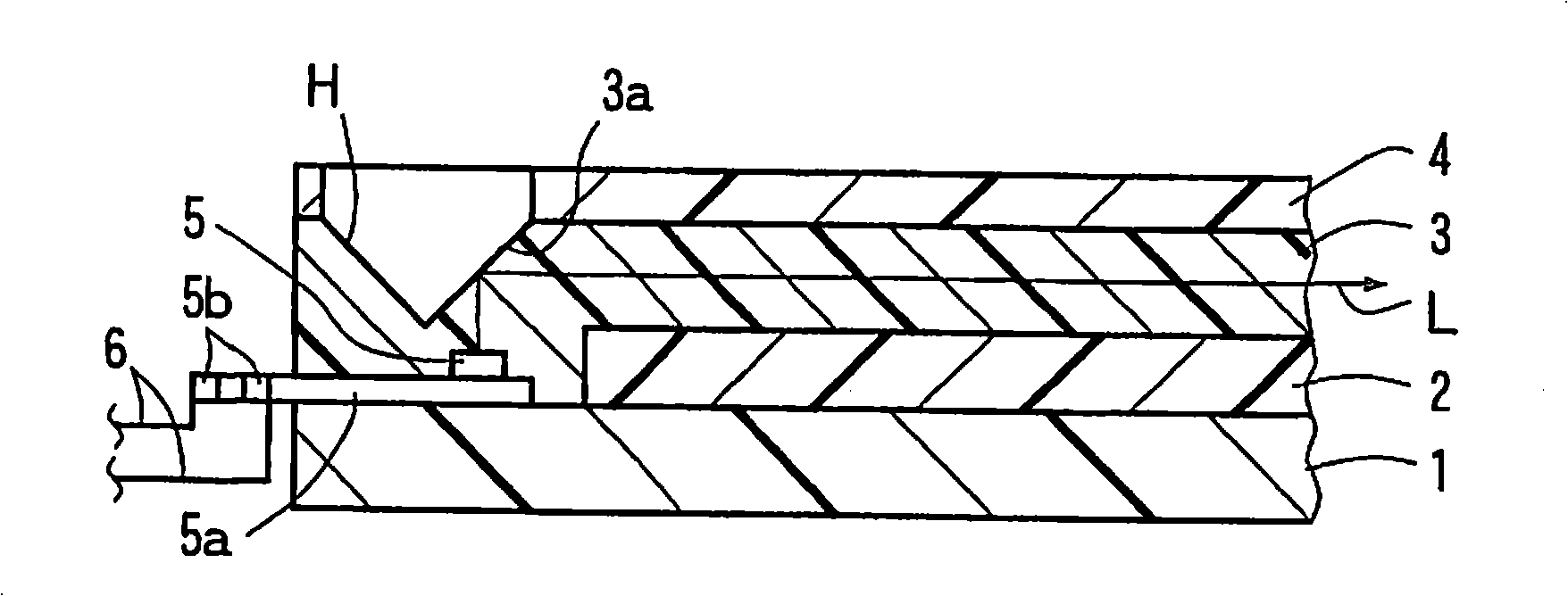
The invention provides an optical waveguide device and method of manufacturing the same. No light path block article exists between the light-emitting element and optical waveguide, wherein, light-emitting elements are provided on the substrate; an under-cladding layer provided on a portion of the upper surface of the substrate except for the light emitting element provision region is provided; and a core covering the light emitting element and the under-cladding layer on the substrate and serving as a path of light emitted from the light emitting element, is formed. The core fixes up the light-emitting element and makes the light generated from self-luminescence elements to directly irradiate in.

Description

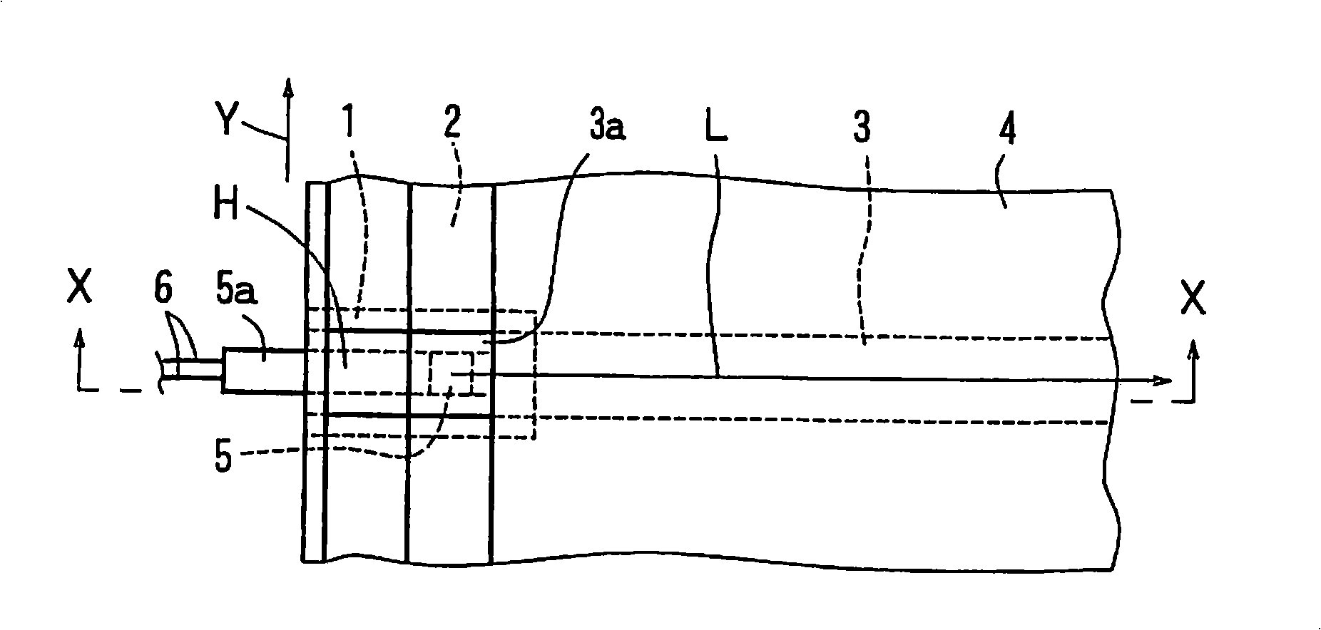
[0001] technology area [0002] The present invention relates to an optical waveguide device widely used in optical communication, optical information processing, and other general optics and a manufacturing method thereof. Background technique [0003] Generally, in an optical waveguide device, light emitted from a light-emitting element is propagated using an optical waveguide (see, for example, US5914709). Figure 5 The optical waveguide device is schematically shown. Figure 5 In the optical waveguide device, an optical waveguide composed of a lower cladding layer 20 , a core layer 30 , and an upper cladding layer 40 is formed on a substrate 10 . Then, the light emitting element 50 is spaced apart from the one end side of the optical waveguide, and the light emitting element 50 is fixed to the substrate 10 via the adhesive A. The light L emitted from the light emitting element 50 enters from one end surface of the core layer 30 of the optical waveguide, passes through the ...

Claims


Application Information

Patent Timeline
Patent Type & Authority Applications(China)
IPC IPC(8): G02B6/122G02B6/13H01L33/54H01L33/56H01L33/62
CPCG02B6/138G02B6/4202G02B6/1221G02B6/12G02B6/42
Inventor 疋田贵巳宗和范
Owner NITTO DENKO CORP
Learn More