Method for flattening wafer surface

A surface planarization and wafer technology, applied in chemical instruments and methods, crystal growth, electrical components, etc., can solve the problem that the wafer edge cannot meet the planarization requirements, and achieve the effect of improving the degree of planarization

Inactive Publication Date: 2009-02-04
SEMICON MFG INT (SHANGHAI) CORP +1
View PDF1 Cites 23 Cited by
  • Summary
  • Abstract
  • Description
  • Claims
  • Application Information

AI Technical Summary

Problems solved by technology

[0005] The present invention is to solve the problem that the edge of the wafer in the prior art cannot meet the planarization requirement

Method used


Image

  • Method for flattening wafer surface
  • Method for flattening wafer surface
  • Method for flattening wafer surface

Examples


Embodiment Construction

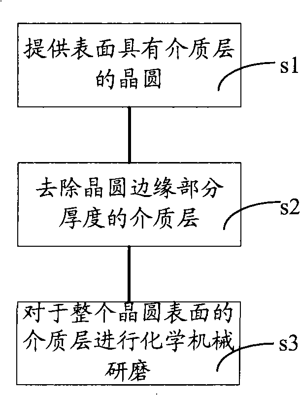
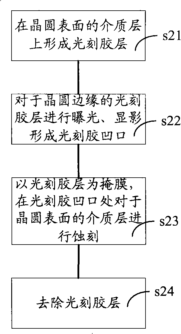
[0018] The essence of the method for planarizing the wafer surface of the present invention is to etch the dielectric layer in the edge region of the wafer to remove a part of the thickness of the dielectric layer before chemically mechanically grinding the dielectric layer on the wafer surface, so as to achieve the desired effect on the wafer after grinding. The purpose of correcting the thickness difference between the dielectric layer in the edge area and the dielectric layer in the center area of ​​the wafer, wherein the edge area is the dielectric layer area where the thickness of the dielectric layer is greater than the depth of the etched through hole after the test piece is ground, and the removal thickness of the dielectric layer is greater than or It is equal to the average thickness difference between the dielectric layer in the central area of ​​the wafer and the dielectric layer in the edge area of ​​the wafer measured by the test piece.

[0019] The method for fla...


PUM

PropertyMeasurementUnit
thicknessaaaaaaaaaa

Abstract

The invention discloses a method for smoothening the surface of a wafer, including the following steps: providing a wafer which is provided with a medium layer on the surface and is composed of a central area and a marginal area surrounding the central area; removing the medium layer at the marginal area; and chemically and mechanically rubbing the whole medium layer on the surface of the wafer; wherein the thickness of the medium layer at the marginal area after being rubbed by a test piece is bigger than the depth of the etched through hole; and the removed thickness of the medium layer at the marginal area is larger than or equal to the average thickness difference tested by a test piece between the medium layer at the central area and the marginal area of the chemically and mechanically rubbed wafer. The method for smoothening the surface of the wafer reduces thickness difference between the medium layer at the central area and the marginal area of the wafer after chemically and mechanically rubbing the surface of the medium layer on the surface of the wafer, thus improving the smoothness of the surface of the wafer.

Description

technical field [0001] The invention relates to a method for flattening the surface of a wafer. Background technique [0002] In the manufacturing process of large-scale integrated circuits and ultra-large-scale integrated circuits, in order to increase the density of components and their operating speed, the components of semiconductor wafers, metal wiring, and even the structure used to isolate the distribution of component trenches need to pass through designed to meet the requirements of various components. However, these elements and structures are often not evenly distributed on the surface of the semiconductor wafer, so there are some dense element areas where elements and structures are denser and loose element areas where elements and structures are sparsely distributed. On the other hand, these elements and structures all have a certain thickness, so the surface of the semiconductor wafer has some ups and downs. Therefore, a planarization step is required. [00...

Claims


Application Information

Patent Timeline
Patent Type & Authority Applications(China)
IPC IPC(8): H01L21/302C30B33/00
Inventor 仇圣棻孙鹏施平高金凤
Owner SEMICON MFG INT (SHANGHAI) CORP
Why Eureka
Try Eureka